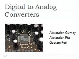
Ben Lester Mike Steele Quinn Morrison Topics Introduction Why Types and Comparisons Successive Approximation ADC example Applications ADC System in the CML12C32 Microcontroller Analog systems are typically what engineers need to analyze ADCs are used to turn analog information into dig ID: 136731
Download Presentation The PPT/PDF document "Analog to Digital Converters (ADC)" is the property of its rightful owner. Permission is granted to download and print the materials on this web site for personal, non-commercial use only, and to display it on your personal computer provided you do not modify the materials and that you retain all copyright notices contained in the materials. By downloading content from our website, you accept the terms of this agreement.
Slide1
Analog to Digital Converters (ADC)
Ben Lester, Mike Steele, Quinn MorrisonSlide2
Topics
Introduction
Why?
Types and Comparisons
Successive Approximation ADC example
Applications
ADC System in the CML-12C32 MicrocontrollerSlide3
Analog systems are typically what engineers need to analyze. ADCs are used to turn analog information into digital data.Slide4
Process
Sampling, Quantification, Encoding
Output States
Discrete Voltage Ranges (V)
0
0.00-1.25
1
1.25-2.50
2
2.50-3.75
33.75-5.0045.00-6.2556.25-7.5067.50-8.7578.75-10.0
Out-put
Binary Equivalent
0
000
1
001
2
010
3
011
4
100
5
101
6
110
7
111Slide5
Resolution, Accuracy, and Conversion time
Resolution – Number of discrete values it can produce over the range of analog values; Q=R/N
Accuracy – Improved by increasing sampling rate and resolution.
Time – Based on number of steps required in the conversion process.Slide6
Comparing types of ADCs
Flash ADC
Sigma-delta ADC
Wilkinson ADC
Integrating ADC
Successive Approximation ConverterSlide7
Flash ADC
Speed: High
Cost: High
Accuracy: LowSlide8
Sigma-delta ADC
Speed: Low
Cost: Low
Accuracy: HighSlide9
Wilkinson ADC
Speed: High
Cost: High
Accuracy: High
Wilkinson Analog Digital Converter (ADC) circuit schematic diagram Slide10
Integrating ADC
Speed: Low
Cost: Low
Accuracy: HighSlide11
Successive Approximation Converter
Speed: High
Cost: High
Accuracy: High but limitedSlide12
Topics
Introduction
Why?
Types and Comparisions
Successive Approximation ADC example
Applications
ADC System in the CML-12C32 MicrocontrollerSlide13
Successive Approximation ADC Example
Mike Steele
Goal:
Find digital value V
in
8-bit ADC
V
in
= 7.65
Vfull scale = 10Slide14
Successive Approximation ADC Example
MSB
LSB
Average high/low limits
Compare to V
in
V
in
> Average MSB = 1 Vin < Average MSB = 0 Bit 7 (Vfull scale +0)/2 = 5 7.65 > 5 Bit 7 = 1Vfull scale = 10, Vin = 7.651 Slide15
Successive Approximation ADC Example
MSB
LSB
Average high/low limits
Compare to V
in
V
in
> Average MSB = 1 Vin < Average MSB = 0 Bit 6 (Vfull scale +5)/2 = 7.5 7.65 > 7.5 Bit 6 = 1Vfull scale = 10, Vin = 7.651 1 Slide16
Successive Approximation ADC Example
MSB
LSB
Average high/low limits
Compare to V
in
V
in
> Average MSB = 1 Vin < Average MSB = 0 Bit 5 (Vfull scale +7.5)/2 = 8.75 7.65 < 8.75 Bit 5 = 0Vfull scale = 10, Vin = 7.651 1 0 Slide17
Successive Approximation ADC Example
MSB
LSB
Average high/low limits
Compare to V
in
V
in
> Average MSB = 1 Vin < Average MSB = 0 Bit 4 (8.75+7.5)/2 8.125 7.65 < 8.125 Bit 4 = 0 Vin = 7.651 1 0 0 Slide18
Successive Approximation ADC Example
MSB
LSB
Average high/low limits
Compare to V
in
V
in
> Average MSB = 1 Vin < Average MSB = 0 Bit 3 (8.125+7.5)/2 = 7.8125 7.65 < 7.8125 Bit 3 = 0 Vin = 7.651 1 0 00 Slide19
Successive Approximation ADC Example
MSB
LSB
Average high/low limits
Compare to V
in
V
in
> Average MSB = 1 Vin < Average MSB = 0 Bit 2 (7.8125+7.5)/2 = 7.65625 7.65 < 7.65625 Bit 2 = 0 Vin = 7.651 1 0 00 0 Slide20
Successive Approximation ADC Example
MSB
LSB
Average high/low limits
Compare to V
in
V
in
> Average MSB = 1 Vin < Average MSB = 0 Bit 1 (7.65625+7.5)/2 = 7.578125 7.65 > 7.578125 Bit 1 = 1 Vin = 7.651 1 0 00 01 Slide21
Successive Approximation ADC Example
MSB
LSB
Average high/low limits
Compare to V
in
V
in
> Average MSB = 1 Vin < Average MSB = 0 Bit 0 (7.65625+7.578125)/2 = 7.6171875 7.65 > 7.6171875 Bit 0 = 1 Vin = 7.651 1 0 00 01 1 Slide22
Successive Approximation ADC Example
11000011
2
= 195
10
8-bits, 2
8
= 256
Digital Output
195/256 = 0.76171875
Analog Input 7.65/10 = 0.765 Resolution (Vmax – Vmin)/2n 10/256 = 0.0391 1 0 00 01 1 VoltageBit Vin = 7.65Slide23
ADC Applications
Measurements / Data Acquisition
Control Systems
PLCs (Programmable Logic Controllers)
Sensor integration (Robotics)
Cell Phones
Video Devices
Audio Devices
t
t
ee*Controller0010010100111011∆te*(∆t)1001001010100101∆tu*(∆t)Slide24
ATD10B8C on MC9S12C32
Presented by
Quinn MorrisonSlide25
MC9S12C32
Block Diagram
ATD 10B8CSlide26
ATD10B8C Block DiagramSlide27
ATD10B8C Key Features
Resolution
8/10 bit (manually chosen)
Conversion Time
7 usec, 10 bit
Successive Approximation ADC architecture
8-channel multiplexed inputs
External trigger control
Conversion modes
Single or continuous sampling
Single or multiple channelsSlide28
ATD10B8C Modes and Operations
Modes
Stop Mode
All clocks halt; conversion aborts; minimum recovery delay
Wait Mode
Reduced MCU power; can resume
Freeze ModeBreakpoint for debugging an application
Operations
Setting up and Starting the A/D Conversion
Aborting the A/D Conversion
ResetsInterruptsSlide29
ATD10B8C External Pins
There Are 12 External Pins
AN7 / ETRIG / PAD7
Analog input channel 7
External trigger for ADC
General purpose digital I/O
AN6/PAD6 – AN0/PAD0
Analog input
General purpose digital I/O
V
RH, VRLHigh and low reference voltages for ADCVDDA, VSSAPower supplies for analog circuitrySlide30
ATD10B8C Registers
6 Control Registers
($0080 - $0085)
Configure general ADC operation
2 Status Registers
($0086, $008B)
General status information regarding ADC
2 Test Registers
($0088 - $0089)
Allows for analog conversion of internal states
16 Conversion Result Registers ($0090 - $009F)Formatted results (2 bytes)1 Digital Input Enable Register ($008D)Convert channels to digital inputs1 Digital Port Data Register ($008F)Contains logic levels of digital input pinsSlide31
ATD10B8C
Control Register 2Slide32
ATD10B8C Control Register 3Slide33
ATD10B8C Control Register 4Slide34
ATD10B8C Control Register 5Slide35
ATD10B8C Single Channel ConversionsSlide36
ATD10B8C Multi-channel ConversionsSlide37
ATD10B8C Status Register 0Slide38
ATD10B8C Status Register 1Slide39
ATD10B8C Results RegistersSlide40
ATD10B8C Results Registers Slide41
ATD10B8C ATD Input Enable RegisterSlide42
ATD10B8C Port Data RegisterSlide43
ATD10B8C Setting up the ADCSlide44
References
Dr. Ume,
http://www.me.gatech.edu/mechatronics_course/
Maxim Integrated Products, AN1870, AN 1870, APP1870, Appnote1870, Appnote
1870
"An Introduction to Sigma Delta Converters."
Die Homepage Der Familie Beis
. 10
June 2008. Web. 27 Sept. 2010.
<http://www.beis.de/Elektronik/DeltaSigma/SigmaDelta.html>.