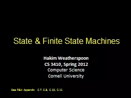
Prof Kavita Bala and Prof Hakim Weatherspoon CS 3410 Spring 2014 Computer Science Cornell University See PampH Appendix B7 B8 B10 B11 Stateful Components Until now is combinatorial logic ID: 617248
Download Presentation The PPT/PDF document "State and Finite State Machines" is the property of its rightful owner. Permission is granted to download and print the materials on this web site for personal, non-commercial use only, and to display it on your personal computer provided you do not modify the materials and that you retain all copyright notices contained in the materials. By downloading content from our website, you accept the terms of this agreement.
Slide1
State and Finite State Machines
Prof. Kavita Bala and Prof. Hakim WeatherspoonCS 3410, Spring 2014Computer ScienceCornell University
See P&H Appendix
B.7
.
B.8
,
B.10
,
B.11 Slide2
Stateful
ComponentsUntil now is combinatorial logicOutput is computed when inputs are present
System has no internal state
Nothing computed in the present can depend on what happened in the past!
Need a way to record dataNeed a way to build stateful circuitsNeed a state-holding deviceFinite State Machines
Inputs
Combinationalcircuit
Outputs
N
MSlide3
Goals for Today
StateHow do we store one
bit?
Attempts at storing (and changing) one bit
Set-Reset LatchD LatchD Flip-FlopsMaster-Slave Flip-FlopsRegister: storing more than one bit, N-bitsBasic Building BlocksDecoders and EncodersFinite State Machines (FSM)How do we design logic circuits with state?Types of FSMs: Mealy and Moore MachinesExamples: Serial Adder and a Digital Door LockSlide4
Goal
How do we store store one bit?Slide5
First Attempt: Unstable Devices
B
A
CSlide6
Second Attempt:
Bistable Devices
A
B
A Simple Device
Stable and unstable equilibria?Slide7
B
R
Third Attempt: Set-Reset Latch
Q
A
S
Can you store a value (with this circuit)?
Can you change its value?Slide8
Third Attempt:
Set-Reset LatchSet-Reset (S-R) Latch
Stores a value Q and
its complement
S
R
Q
0
0
0
1
1
0
1
1
S
R
Q
0
0
0
1
1
0
1
1
S
R
Q
A
B
OR
NOR
0
0
0
1
0
1
1
0
1
0
1
0
1
1
1
0Slide9
Third Attempt:
Set-Reset LatchSet-Reset (S-R) Latch
Stores a value Q and
its complement
S
R
Q
0
0
0
1
1
0
1
1
S
R
Q
0
0
0
1
1
0
1
1
S
R
Q
A
B
OR
NOR
0
0
0
1
0
1
1
0
1
0
1
0
1
1
1
0
S
R
Q
Slide10
Takeaway
Set-Reset (SR) Latch can store one bit and we can change the value of the stored bit. But, SR Latch has a forbidden state.Slide11
Next Goal
How do we avoid the forbidden state of S-R Latch?Slide12
Fourth Attempt: (
Unclocked) D
Latch
Fill in the truth table?
D
S
R
Q
Q
D
D
Q
0
1
D
Q
0
1
S
R
Q
A
B
OR
NOR
0
0
0
1
0
1
1
0
1
0
1
0
1
1
1
0Slide13
Takeaway
Set-Reset (SR) Latch can store one bit and we can change the value of the stored bit. But, SR Latch has a forbidden state.(Unclocked
) D Latch can store and change a bit like an SR Latch while avoiding the forbidden state.Slide14
Next Goal
How do we coordinate state changes to a D Latch?Slide15
Clocks
Clock
helps coordinate state changes
Usually generated
by an oscillating crystalFixed period; frequency = 1/period
period
high
low
1
0
falling
edge
rising
edge
clock
period
clock
high
clock
low
rising
edge
falling
edgeSlide16
Clock Disciplines
Level sensitiveState changes when clock is high (or low)
Edge triggered
State changes at clock edge
positive edge-triggered
negative
edge-triggeredSlide17
Clock Methodology
Clock MethodologyNegative edge, synchronous
Edge-Triggered: Signals must be stable near falling clock edge
Positive edge synchronous
clk
compute
save
t
setup
t
hold
compute
save
compute
t
combinationalSlide18
Fifth Attempt: D Latch with Clock
S
R
D
Q
Slide19
Fifth Attempt: D Latch with Clock
S
R
D
clk
Q
clk
D
Q
0
0
0
1
1
0
1
1
clk
D
Q
0
0
0
1
1
0
1
1
Fill in the truth tableSlide20
clk
D
Q
0
0
0
1
1
0
1
1
clk
D
Q
0
0
0
1
1
0
1
1
Fifth Attempt: D Latch with Clock
S
R
D
clk
Q
S
R
Q
0
0
Q
hold
0
1
0
1
reset
1
0
1
0
set
1
1
forbidden
S
R
Q
0
0
Q
hold
0
1
0
1
reset
1
0
1
0
set
1
1
forbidden
clk
D
Q
0
0
0
1
1
0
1
1
clk
D
Q
0
0
0
1
1
0
1
1
Fill in the truth tableSlide21
Fifth Attempt: D
Latch with Clock
S
R
D
clk
Q
clk
D
Q
0
0
0
1
1
0
1
1
clk
D
Q
0
0
0
1
1
0
1
1
clk
D
Q
Fill in the truth tableSlide22
Sixth Attempt: Edge-Triggered D Flip-Flop
D
Q
D
Q
L
L
clk
D
X
Q
c
X
c
Q
D
clk
0
0
1
0
1
Activity#1: Fill in timing graph and values for X and QSlide23
Takeaway
Set-Reset (SR) Latch can store one bit and we can change the value of the stored bit. But, SR Latch has a forbidden state.(Unclocked) D Latch can store and change a bit like an SR Latch while avoiding a forbidden state.
An Edge-Triggered D Flip-Flip (aka Master-Slave D Flip-Flip) stores one bit. The bit can be changed in a synchronized fashion on the edge of a clock signal.Slide24
Next Goal
How do we store more than one bit, N bits?Slide25
Registers
RegisterD flip-flops in parallel
shared clock
extra clocked inputs:
write_enable, reset, …
clk
D0
D3
D1
D2
4
4
4-bit
reg
clkSlide26
Takeaway
Set-Reset (SR) Latch can store one bit and we can change the value of the stored bit. But, SR Latch has a forbidden state.(Unclocked) D Latch can store and change a bit like an SR Latch while avoiding a forbidden state.
An Edge-Triggered D Flip-Flip (aka Master-Slave D Flip-Flip) stores one bit. The bit can be changed in a synchronized fashion on the edge of a clock signal.
An
N-bit register stores N-bits. It is be created with N D-Flip-Flops in parallel along with a shared clock.Slide27
An Example: What will this circuit do?
4
-bit
reg
Clk
Decoder
+1
4
4
4
16
4Slide28
Decoder Example:
7-Segment LED 7-Segment LEDphotons emitted when electrons fall into holes
d7
d6
d5
d4
d3
d2
d1
d0Slide29
Decoder Example: 7-Segment
LED Decoder
3 inputs
encode 0 – 7 in binary
7
outputs
one for each LED
7LED decodeSlide30
b2
b1
b0
d6
d5
d4
d3
d2
d1
d0
0
0
0
0
0
1
0
1
0
0
1
1
1
0
0
1
0
1
1
1
0
1
1
1
7 Segment LED Decoder Implementation
d0
d1
d2
d3
d4
d5
d6
b2
b1
b0
d6
d5
d4
d3
d2
d1
d0
0
0
0
0
0
1
0
1
0
0
1
1
1
0
0
1
0
1
1
1
0
1
1
1Slide31
7 Segment LED Decoder Implementation
d0
d1
d2
d3
d4
d5
d6
b2
b1
b0
d6
d5
d4
d3
d2
d1
d0
0
0
0
0
0
1
0
1
0
0
1
1
1
0
0
1
0
1
1
1
0
1
1
1
1
1
1
0
1
1
1
1
0
0
0
0
0
1
0
1
1
1
0
1
1
1
1
0
1
0
1
1
1
0
0
1
1
0
1
1
1
0
1
1
1
0
1
1
1
1
1
1
0
1
0
0
0
0
1
1Slide32
Basic Building Blocks We have Seen
binary
encoder
2
N
N
binary
decoder
N
2
N
Multiplexor
N
M
N
N
N
N
. . .
0
1
2
2
M
-1Slide33
Encoders
1
2
3
4
5
6
7
0
encoder
N
. . .
. . .
Log
2
(N) outputs wires
N Input wires
e.g. Voting:
Can only vote for one out of N
candidates, so
N inputs.
B
ut can encode vote efficiently
with binary encoding.Slide34
Example Encoder
Truth Table
a
b
1
c
d
2
3
4
o
1
A 3-bit
encoder
with 4 inputs
for simplicity
a
b
c
d
0
0
0
0
1
0
0
0
0
1
0
0
0
0
1
0
0
0
0
1
o
0
o
1
o
2Slide35
Basic Building Blocks Example: Voting
Ballots
The 3410
optical scan
vote reader
machine
detect
enc
8
3
7
7LED
decodeSlide36
Recap
We can now build interesting devices with sensorsUsing combinatorial logicWe can also store data values (aka Sequential Logic)
In state-holding elements
Coupled with
clocksSlide37
Administrivia
Make sure to go to your
Lab Section
this weekCompleted Lab1 due before winter break, Friday, Feb 14thNote, a Design Document is due when you submit Lab1 final circuitWork aloneHomework1 is out
Due a week before prelim1, Monday, February 24thWork on problems incrementally, as we cover them in lectureOffice Hours for help
Work aloneWork alone,
BUT use your resourcesLab Section, Piazza.com, Office Hours
Class notes, book, Sections, CSUGLabSlide38
Administrivia
Check online syllabus/schedule http
://
www.cs.cornell.edu/Courses/CS3410/2014sp/schedule.html
Slides and Reading for lecturesOffice HoursHomework and Programming AssignmentsPrelims (in evenings): Tuesday, March 4th Thursday, May
1th
Schedule is subject to changeSlide39
Collaboration, Late, Re-grading Policies
“Black Board” Collaboration PolicyCan discuss approach together on a “black board”
Leave and write up solution independently
Do not copy solutions
Late PolicyEach person has a total of four “slip days”Max of
two slip days
for any individual assignmentSlip days deducted first
for any late assignment, cannot selectively apply slip days
For projects, slip days are deducted from all partners 25% deducted per day late after slip days are exhausted
Regrade policySubmit written request to lead TA, and lead TA will pick a different grader
Submit another written request, lead TA will regrade directly
Submit yet another written request for professor to regrade.Slide40
Goals for Today
StateHow do we store
one
bit?
Attempts at storing (and changing) one bitSet-Reset LatchD LatchD Flip-FlopsMaster-Slave Flip-FlopsRegister: storing more than one bit, N-bitsBasic Building Blocks
Decoders and EncodersFinite State Machines (FSM)How do we design logic circuits with state?Types of FSMs: Mealy and Moore Machines
Examples: Serial Adder and a Digital Door LockSlide41
Finite State MachinesSlide42
Next Goal
How do we design logic circuits with state?Slide43
Finite State Machines
An electronic machine which hasexternal inputsexternally visible outputsinternal stateOutput and next state depend oninputscurrent stateSlide44
Abstract Model of FSM
Machine is M = ( S, I, O,
)
S
: Finite set of statesI: Finite set of inputsO: Finite set of outputs: State transition functionNext state depends on present input and present stateSlide45
Automata Model
Finite State Machine
inputs from external world
outputs to external world
internal statecombinational logic
Next
State
Current State
Input
Output
Registers
Comb.
LogicSlide46
FSM Example
Legend
state
input
/
output
start
state
A
B
C
D
down
/
on
up
/
off
down
/
on
down
/
off
up
/
off
up
/
off
down
/
off
up
/
off
Input:
up
or
down
Output:
on
or
off
States:
A
,
B
,
C
, or
DSlide47
FSM Example
Legend
state
input
/
output
start
state
A
B
C
D
down
/
on
up
/
off
down
/
on
down
/
off
up
/
off
up
/
off
down
/
off
up
/
off
Input: =
up
or =
down
Output: =
on
or =
off
States: =
A
, =
B
, =
C
, or =
DSlide48
FSM Example
Legend
S
1
S
0
i
0
i
1
i2…/
o0o
1o2
…
S
1
S
0
00
01
10
11
1
/
1
0
/
0
1
/
1
1
/
0
0
/
0
1
/
0
0
/
0
0
/
0
Input:
0
=up or
1
=down
Output:
1
=on or
1
=off
States:
00
=A,
01
=B,
10
=C, or
11
=DSlide49
General Case:
Mealy Machine Outputs and next state depend on both
current state and input
Mealy Machine
Next State
Current State
Input
Output
Registers
Comb.
LogicSlide50
Moore Machine
Special Case: Moore Machine
Outputs depend only on current state
Next
State
Current State
Input
Output
Registers
Comb.
Logic
Comb.
LogicSlide51
Moore Machine FSM Example
Legend
state
out
input
start
out
A
off
B
on
C
off
D
off
down
up
down
down
up
up
down
up
Input:
up
or
down
Output:
on
or
off
States:
A
,
B
,
C
, or
DSlide52
Mealy Machine FSM Example
Legend
state
input
/
output
start
state
A
B
C
D
down
/
on
up
/
off
down
/
on
down
/
off
up
/
off
up
/
off
down
/
off
up
/
off
Input:
up
or
down
Output:
on
or
off
States:
A
,
B
,
C
, or
DSlide53
Activity#2: Create a Logic Circuit for a Serial
AdderAdd two infinite input bit streamsstreams are sent with least-significant-bit (lsb)
first
How many states are needed to represent FSM?
Draw and Fill in FSM diagram
…10110
…01111
…00101
Strategy
:
(1) Draw a state diagram (e.g. Mealy Machine)
(2) Write output and next-state tables
(3) Encode states, inputs, and outputs as bits
(4) Determine logic equations for next state and outputsSlide54
FSM: State Diagram
states
:
Inputs: ??? and ???Output: ???.
…10110
…01111
…00101Slide55
FSM: State Diagram
states
:
Inputs: ??? and ???Output: ???.
S0
S1
__
/
_
__
/
_
__
/
_
__
/
_
__
/
_
__
/
_
__
/
_
__
/
_
…10110
…01111
…00101Slide56
FSM: State Diagram
??
??
Current state
?
Next state
(2) Write down all input and state combinations
S0
S1
__
/
_
__
/
_
__
/
_
__
/
_
__
/
_
__
/
_
__
/
_
__
/
_Slide57
FSM: State Diagram
??
??
Current state
?
Next state
(3) Encode states, inputs, and outputs as bits
S0
S1
__
/
_
__
/
_
__
/
_
__
/
_
__
/
_
__
/
_
__
/
_
__
/
_Slide58
FSM: State Diagram
??
??
Current state
?
Next state
(4) Determine logic equations for next state and outputsSlide59
Summary
We can now build interesting devices with sensorsUsing combinational logicWe can also store data valuesStateful circuit elements (D Flip Flops, Registers, …)
Clock to synchronize state changes
State Machines or Ad-Hoc Circuits