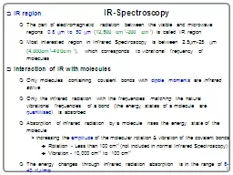
PDF-Spectroscopy of Covalently Functionalized graphene

Author : marina-yarberry | Published Date : 2017-03-30

TowhomcorrespondenceshouldbeaddressedEmailhaddonucreduReceivedforreview06152010PublishedonWeb08252010

Presentation Embed Code

Download Presentation

Download Presentation The PPT/PDF document "Spectroscopy of Covalently Functionaliz..." is the property of its rightful owner. Permission is granted to download and print the materials on this website for personal, non-commercial use only, and to display it on your personal computer provided you do not modify the materials and that you retain all copyright notices contained in the materials. By downloading content from our website, you accept the terms of this agreement.

Spectroscopy of Covalently Functionalized graphene: Transcript


TowhomcorrespondenceshouldbeaddressedEmailhaddonucreduReceivedforreview06152010PublishedonWeb08252010. Piner Luigi Colombo and Rodney S Ruoff Department of Mechanical Engineering and the Texas Materials Institute The Uni ersity of Texas at Austin Austin Texas 787120292 2009 NNIN REU Intern at The Uni ersity of Texas at Austin Austin Texas 787120292 nanoribbons. : influence of edge passivation and uniaxial strain. Benjamin O. . Tayo. Physics Department, Pittsburg State University Pittsburg, KS. 1. WSU Physics Seminar. Wichita, KS. November 12, 2014. Ozkans. ’. laboratory in UC-Riverside to perform defect analysis and surface metrology of large-area CVD-graphene sheets. This method utilizes the quenching of fluorescence from dye molecules by graphene via resonant energy transfer to increase the visibility of graphene on a glass substrate. A large-area fluorescence montage image of the dyed graphene sample is collected and processed to identify the graphene and indicate the graphene layer thickness throughout the entire graphene sheet. Furthermore, chemically functionalized (doped with fluorine) parts of graphene film is visualized using the same technique. The emission of the dye is quenched to a different extent by fluorinated and pristine graphene, which provides the fluorescence-imaging contrast essential for this method. The regions with pristine graphene appear darker on the fluorescence images than the regions with fluorinated graphene, enabling large-scale mapping of the functionalized regions in CVD grown graphene sheets. Complex circular patterned regions of doped and pristine graphene regions are resolved with great accuracy. This method is posed for widespread adoption by graphene manufacturers as a basis for facile and high throughput metrology of large scale graphene sheets. Finally, this work featured as cover articles in . Janice E. . Reutt-Robey. , University of Maryland College Park, DMR 0520471. A microscope technique called “Kelvin probe microscopy” (KPM) is used to map the differences in the electrical potential on the surface of graphene on silicon carbide, shown here as different colors. KPM identifies single layer graphene (SLG), bilayer graphene (BLG), and two types of interfacial layer (IL1 and IL2). . Fei. Yu and . Vikram. . Kuppa. School of Energy, Environmental, Biological and Medical Engineering. College of Engineering and Applied Science. University of Cincinnati. APS . March . Meeting 2012, Boston. Kevin Babb & Petar Petrov. Physics 141A Presentation. March 5, 2013. What is a Nanowire?. “One-dimensional” structure. Diameter: 1-100 nanometers (10. -9. m). Length: microns (10. -6. m). Exhibits crystal structure. Grayton. . Giesman. , Nick Grosenbacher, Joseph . Nemec. Background. Graphene. is a material made of carbon atoms in sheet . form.. 1. It is so thin that it is often considered two-dimensional.. It is “widely cited as the strongest material ever created on a per-weight basis, but it also has incredibly high electrical conductivity. Institute for Nuclear Problems, Belarus State University, Belarus. The XII-. th. International School-Seminar.  . The Actual Problems of . Microworld. Physics . Gomel, Belarus, July 22 - August 2, 2013. Piet Van Duppen. ISOLDE CERN, Switzerland. IKS-. K.U.Leuven. , Belgium. K.U. Leuven. University of Western Scotland, U.K. - . K.U.Leuven. , Belgium - SCK-CEN-Mol, Belgium - . U.Gent. , Belgium - . Commenius. 369 A packaged and wire-bonded die containing 64 nanoelectromechanical accelerometers made from suspended double-layer graphene ribbons with attached silicon proof masses. Credit: Springer Nature LtdN from NANOTECHNOLOGY capacitors batteries flexible electronics composites filtrations sensors etcGraphene is a high aspect ratio nanocarbon material x0000 50001 possibleCost-efficient volume scalable g 2. Nuclear Magnetic Resonance Spectroscopy. After hydrogen, the most useful atom providing information is carbon-13.. The . overall intensity of a . 13. C signal is about 6400 . times . less than the intensity of an . applications . Graphene. is a one-atom-thick planar sheet of . sp. 2. -bonded. . carbon. atoms that are densely packed in a honeycomb crystal lattice. Molecular structure . . . of graphene. High resolution transmission electron microscope images. Dr. Satyanarayan Dhal. Lecture-24. Why Graphene ?. Discovery : 2004, . Geim. and . Nosovelov. at Manchester University. Extraordinary electronic, chemical, mechanical, thermal and optical properties. .

Download Document

Here is the link to download the presentation.
"Spectroscopy of Covalently Functionalized graphene"The content belongs to its owner. You may download and print it for personal use, without modification, and keep all copyright notices. By downloading, you agree to these terms.

Related Documents