/
Evolution of the Intel Architecture Evolution of the Intel Architecture

Evolution of the Intel Architecture - PowerPoint Presentation

okelly
okelly . @okelly
Follow
65 views
Uploaded On 2023-11-11

Evolution of the Intel Architecture - PPT Presentation

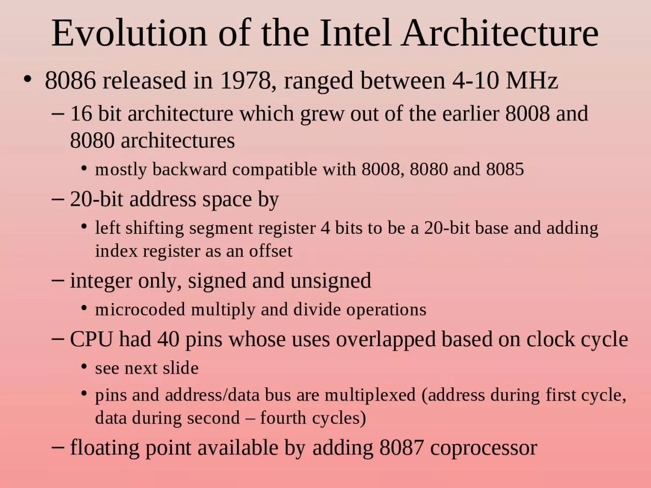
8086 released in 1978 ranged between 410 MHz 16 bit architecture which grew out of the earlier 8008 and 8080 architectures mostly backward compatible with 8008 8080 and 8085 20bit address space by ID: 1031009

micro control instruction instructions control micro instructions instruction address memory cycle cache data branch unit register buffer mbr stations

Share:

Link:

Embed:

Download Presentation from below link

Download Presentation The PPT/PDF document "Evolution of the Intel Architecture" is the property of its rightful owner. Permission is granted to download and print the materials on this web site for personal, non-commercial use only, and to display it on your personal computer provided you do not modify the materials and that you retain all copyright notices contained in the materials. By downloading content from our website, you accept the terms of this agreement.


Presentation Transcript

1. Evolution of the Intel Architecture8086 released in 1978, ranged between 4-10 MHz16 bit architecture which grew out of the earlier 8008 and 8080 architecturesmostly backward compatible with 8008, 8080 and 808520-bit address space by left shifting segment register 4 bits to be a 20-bit base and adding index register as an offsetinteger only, signed and unsignedmicrocoded multiply and divide operationsCPU had 40 pins whose uses overlapped based on clock cycle see next slidepins and address/data bus are multiplexed (address during first cycle, data during second – fourth cycles)floating point available by adding 8087 coprocessor

2.

3. Notes:3: add base address and offset5: 4-item instruction buffer (not for prefetching but because instruction lengths vary)10: address bus11 & 12: data and control buses

4. Addressing Modes and Execution TimeEach mode is listed as two numbers1st for mov instruction, 2nd for ALURegister-register: 2, 3Register-immediate: 4, 4Register-memory: 8+EA, 9+EAMemory-register: 9+EA, 16+EAMemory-immediate: 10+EA, 17+EAEA = time to compute effective address which ranges from 5 to 12 cyclesmultiply ranged from 70-160, divide from 80-190For jump instructions: 11 (unconditional, no label), 15 (unconditional, labeled), 16 (conditional, labeled)

5. 80286Introduced in 1982address and data bus and pins separated (no longer multiplexed)protection capabilities to detect memory violationstwo modes: real mode and protected mode (used to permit access to larger memory spaces, up to 4GB)this is because the 286 was designed for multiuser and multitasking systems (even though MS DOS and early versions of Windows were not)ranged from 4-25 MHzperformance averaged CPI of about 5still required a math coprocessor for FP (80287)

6.

7. 80386Released in 1985Extended the 286 architecture to 32 bitsall registers retained but “E” versions added to add the extra 16 bitsThird mode added (virtual mode multitasking)added paging translation unit for virtual memory address translationAdded several new built-in data types: char, string, long int, boolean, pointerstill required math coprocessor for FPClock rates ranged from 12 MHz to 40 MHz

8.

9. 486 ProcessorAdded a pipeline (see next 2 slides)Added floating point functional unitno longer needed the math coprocessorFP unit has its own bus to connect to FP registersfunctional unit provided a degree of parallel processing in that while FP operations were executed, the pipeline would continue to fetch and execute integer operationsAdded an atomic operation to better implement synchronizationContained 8KB combined instruction/data cache later expanded to 16KBClock rates range from 33 MHz to 100 MHz

10. The 486 Pipeline5 stagesFetch 16 bytes worth of instructionmay be 1 instruction, part of 1 instruction, multiple instructionsDecode stage 1 – examine 16 bytes to identify whole instructionif buffer does not contain entire instruction, stall pipeline and continue fetching instructiondivide 16 bytes into instruction(s) (find the end of each instruction)Decode stage 2 – decode the next instructionincludes fetching operands from registersExecution – ALU operations, branch operations, cache (mov) instructionsmay take multiple cycles if ALU operation requires multiple cycles (*, /, FP) or requires 1 (or more) memory accessesfurther stalls needed if memory access is a cache missWrite result of load or ALU operation to register

11. 486 DifficultiesStalls arise for numerous reasons17 byte long instructions require 2 instruction fetch stagesALU memory-register/memory-immediate takes at least 1 additional cyclepossibly two if memory item is both source and destinationsuch a situation stalls instructions in the decode 2 stageor if there is a cache missComplex addressing modes can cause stallspointer accessing (indirect addressing) takes 2 memory accessesscaled addressing mode involves both a shift and an addagain, stalls occur in the decode 2 stageBranch instructions have a 3 cycle penalty branches are computed in the EX stage (4th stage) some loop operations take more than 1 cycle to compute adding a further stall

12. 486 ExamplesExample 1:three data movements, no stallsExample 2: data hazard, 1 cycle of stallExample 3:branch penalty

13. 486 Overall Architecture

14. Pentium ArchitectureSummarizing problems with the 486 pipelinevariable length instructions, variable complexity of operations, memory-register ALU operations, indirect addressingto improve performance using RISC features, Pentium (586) architects needed to rethink things while still implementing backward compatibilityCISC architectures handle the fetch-execute cycle through a microprogrammed control unita microprogram consists of a sequence of microinstructions, each being of equal length and taking 1 clock cycle (usually) to executeRe-implement the pipeline as followscontinue to use an instruction fetch unit to fill a buffer with instructionsuse a separate decode unit to identify each instruction and decode it into microcodeissue microinstructions to a pipeline

15. Control and Micro-OperationsAn example architecture is shown to the rightEach of the various connections is controlled by a particular control signalMBR to the AC controlled with signal C11PC to MAR by C2AC to ALU C7note that this figure is incompleteA microprogram is a sequence of micro-operationsthis is not an x86 architecture!

16. ExampleConsider a CISC instruction such as Add R1, XX copied into MAR and a memory read signaleddatum returned across data bus to MBRadder sent values in R1 and MBR, adding the two, storing result back into R1This sequence can be written in terms of micro-operations as:t1: MAR  (IR (address) )t2: MBR  Memoryt3: R1  (R1) + (MBR)t3: Acc  (R1) + (MBR)t4: R1  (Acc)Each micro-operation is handled by one or more control signalsFor instance, MBR  Memory is C5t1 – t5 are clock cycles, eachmicroinstruction executes inseparate clock cycles

17. Control Memory...Jump to Indirect or Execute...Jump to Execute...Jump to FetchJump to Op code routine...Jump to Fetch or Interrupt...Jump to Fetch or InterruptFetch cycle routineIndirect Cycle routineInterrupt cycle routineExecute cycle beginAND routineADD routineEach micro-program consists of one or more micro-instructions, each stored in a separate entry of the control memoryThe control memory itself is firmware, a program stored in ROM, that is placed inside of the control unitNote: each micro-program ends with a branch to the Fetch, Interrupt, Indirect or Execute micro-program

18. Example of Three Micro-ProgramsFetch: t1: MAR  (PC) C2 t2: MBR  Memory C0, C5, CR PC  (PC) + 1 C* t3: IR  (MBR) C4Indirect: t1: MAR  (IR (address) ) C8 t2: MBR  Memory C0, C5, CR t3: IR(address)  (MBR (address) ) C4Interrupt: t1: MBR  (PC) C1 t2: MAR  save address C* PC  routine address C* t3: Memory  (MBR) C12, CWCR – Read control to system busCW – write control to system busC0 – C12 refers to the previous figure C* are signals not shown in the figure

19. Horizontal vs. Vertical Micro-InstructionsMicro-instruction AddressFunction CodesJump ConditionInternal CPU Control SignalsMicro-instruction AddressJump ConditionSystem BusControl SignalsHorizontal micro-instructions contain 1 bit for every control signal controlled by the control unitVertical micro-instructions use function codes that need additional decodingThis micro-instruction requires 1 bit for every control line, it is longer than the vertical micro-instruction and therefore takes more space to store, but does not require additional time to decode by the control unitMicro-instruction address points to a branch in the control memory and is taken if the condition bit is true

20. Micro-programmed Control Unit

21. ContinuedDecoder analyzes IRdelivers starting address of op code’s micro-program in control store address placed in the to a micro-program counter (here, called a Control Address Register)Loop on the followingsequencer signals read of control memory using address in microPCitem in control memory moved to control buffer registercontents of control buffer register generate control signals and next address informationif the micro-instructions are vertical, decoding is required heresequencer moves next address to control address register next instruction (add 1 to current)jump to new part of this microprogramjump to new machine routine

22. Pentium ArchitecturesPentium I released 1993upgraded to 64-bit data bussuperscalar 5-stage pipeline (2 parallel pipelines)branch speculation addedseparate instruction and data catchesFP portion of the processor had an infamous bug requiring the entire CPU be replaced!Pentium II released 1995added L2 cachePentium III released 1999both PII and PIII used 14-stage pipelinesPentium IV released 2000superscalar expanded to 3 parallel pipelines21-31 stage pipeline

23. Pentium IV: RISC featuresRISC features implemented on microinstructions instead of machine instructionsMicroinstruction-level pipeline Dynamically scheduled micro-operationsReservation stations (128) Multiple functional units (7)Branch speculation via branch target bufferspeculation at micro-instruction levelinstead of an ROB, decisions made at the reservation stations miss-speculation causes reservation stations to flush their contentscorrect speculation causes reservation stations to forward results to registers/store unitstrace cache used (discussed shortly)

24. Pentium II-III PipelineIF unit: 3 stagesID unit: 2 stagesIssue unit: 2 stagesup to 3 microinstructions issued per cycleregister renaming occurs here instructions sent to reservation stationExecution units: 1-32 stages 1 for int, up to 32 for FPWrite back: 3 stagesCommit: 3 stagesup to 3 microinstructions can commit in any cycle

25. Pentium IV Overall Architecture

26. Specifications7 functional units:2 simple ALUs (add, compare, shift) – ½ cycle execution to accommodate up to 2 micro-operations per cycle1 complex ALU (integer multiplication and division) – multicycle, pipelined1 load unit and 1 store unit – including address computation1 FP move (register to register move and convert)1 FP arithmetic unit (+, -, *, /) – multicycle, pipelined, some SIMD execution permitted on these units128 registers for renamingreservation stations are used rather than a re-order buffer instructions must wait in reservation stations longer than in Tomasulo’s version, waiting for speculation results

27. Trace CacheInstruction cachecaches blocks of instructions recently executed togetherTrace cache encodes branch behavior implicitlyMiss-speculated instructions would be discarded from the cachestores microinstructions (not machine instructions)Combining a trace cache and branch target buffer minimizes microinstruction fetch and decodingas long as the microinstructions remain in the trace cacheMiss-predictions at the microinstruction level are far rarer than miss-predictions at the machine level

28. Source of StallsProcess breaks down as followsin the issue stagebranch miss-predictionscache misses, particularly trace cache missreservation stations fulllimited number of entries in the commit bufferless than 3 instructions fetched in 1 cycleless than 3 microinstructions can be issued at the timeat the commit stage branch miss-predictionsinstructions not ready to commit yetbranch computation not yet available

29. ContinuedMiss-prediction of microinstruction are very infrequent (about .8% for int, .1% for FP)FP are often more predictable because they involve a lot of for loopsmachine language level miss-speculation between .1% and 1.5%Trace cache has nearly a 0% miss rateL1 and L2 data caches have miss rates of around 6% and .5% respectivelymachine’s effective CPI ranges from around 1.2 to 5.85 with an average of around 2.2 machine instructions, not micro-operations

30. Intel Core (iCore)Multi-core processors (started with 2 cores)originally released with two cores where one was disabledSame basic architecture as Pentium III but with lower clock rates, this was offset by several new innovationsissue up to 4 microinstructions at a timemore efficient decode stagesusing macro-ops which attempts to combine two micro-instructions into a single one such as a compare and conditional branch more efficient execution unitsone cycle throughput due to pipelined ALU units (previously had a 2-cycle throughput)larger caches and busesno SMT processing (developed for Pentium IV)lower power consumption (needed when there are multiple cores)iCore has released processors of 1, 2, 4 and 6 cores

31. Intel Core i7Aggressive out of order speculationpipeline reduced from 31 to 14 stagesInstruction fetch unitretrieves 16 bytes to decodefeeds a queue that can store up to 18 instructions at a timemultilevel branch target buffer, return address stack for speculationmiss-predictions cause a penalty of about 15 cycles32 KB instruction cacheif a loop is detected that contains fewer than 28 instructions or 256 bytesthese instructions will remain in a buffer to repeatedly be issued (rather than repeated instruction fetches)

32. ContinuedDecoding converts machine instructions into microcode using any of four decoderssimple micro-operation instructions (2 each)complex micro-operation instructions (2 each)Instruction issue can issue up to 6 micro-operations per cycle to36 centralized reservation stations 6 functional units including 1 load and 2 store units that share a memory buffer connected to 3 different data caches

33. i7 Architecture

34. i7 PerformanceCPI for various SPEC06benchmarksAverage CPI is 1.06 forinteger programsand .89 for FP (machineinstructions, not micro-instructions)i7 susceptible to miss-speculation resulting in “wasted” workUp to 40% of the total work that goes into Spec 06 benchmarks is wastedWaste also arises from cache misses (10 cycles or more lost with an L1 miss, 30-40 for L2 misses and as much as 135 for L3 misses)

35. Multicore ProcessorsEach core is a separate processor with its own registers, ALU, control unit, local bus, and L1 cacheL2 cache is shared among all coresL3 off chip may be addedperformance of multicore processors shown belowspeedup is close to but not always linear to the number of cores

36. A Balancing ActImproving one aspect of our processor does not necessarily improve performanceit might actually harm performancelengthening pipeline depth, increasing clock speed in the P4 without adding reservation stations or using a trace cache degrades performancestalls arise at issue stage due to needing more instructions to issuecache misses have greater impact when the clock speed is increasedwithout accurate branch prediction and speculation hardware, stalls from miss-predicted branches can have a tremendous impact on performancewe saw this in both the ARM and i7 processors

37. ContinuedAs clock speeds increasestalls from cache misses create a bigger impact on CPIlarger caches and cache optimization techniques are neededTo support multiple issue of instructionsneed larger cache-to-processor bandwidthIncreasing instruction issue raterequires a proportional increase in the number of reservation stations and reorder buffer size