Explore
Featured
Recent
Articles
Topics
Login
Upload
Featured
Recent
Articles
Topics
Login
Upload
Search Results for 'Wafer-Silicon'
Wafer-Silicon published presentations and documents on DocSlides.
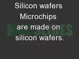
Silicon wafers Microchips are made on silicon wafers.
by calandra-battersby
Silicon wafer. www.guardian.co.uk. http://. mrsec...
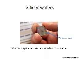
Silicon wafers Microchips are made on silicon wafers.
by faustina-dinatale
Silicon wafer. www.guardian.co.uk. http://. mrsec...
Silicon Wafer Committee Europe
by mitsue-stanley
Werner Bergholz, Jacobs University Bremen. Friedr...
The silicon substrate and adding to
by cheryl-pisano
it—Part 1. Explain . how single crystalline Si ...
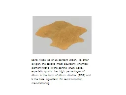
Sand. Made up of 25 percent silicon, is, after oxygen, the
by marina-yarberry
After procuring raw sand and separating the silic...
Silicon Wafer Japan TC Chapter Liaison Report
by alexa-scheidler
For NA Silicon Wafer TC Chapter Meeting. In conju...
Sorenson
by giovanna-bartolotta
. 1. Semiconductor Manufacturing Technology: . S...
Microchannel
by min-jolicoeur
cooling - Update. 07 Sep 2010. 1. G. Nüßle. Ou...
Hazelnut Coffee/Wafers
by celsa-spraggs
By Taylor . Vesel. Hazelnut Coffee, a flavor for ...
Hazelnut Coffee/Wafers
by natalia-silvester
By Taylor . Vesel. Hazelnut Coffee, a flavor for ...
ABC130 Wafer Probe
by test
Peter W Phillips. 12/03/2014. ABC130 Wafer Probe....
EELE 414 – Introduction to VLSI Design
by trinity
Module #4 – CMOS Fabrication. Agenda. CMOS Fabri...
Status of LGAD RD50 projects at CNM
by callie
Outline. Gallium Implantation to Enhance the Radia...
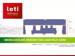
Micro-cooling devices for
by eatsui
LHCb. . Velo. CERN. . 240µm. 260µm. LETI3S ....
Introductio n : The
by test
Genesis Allocation Committee received a request f...
Presented
by alexa-scheidler
By:. Martin . Friedl. Jeremy . Miller. Michael . ...
Introductio
by luanne-stotts
n. : . The . Genesis Allocation Committee receive...
Presentation on
by giovanna-bartolotta
SGS, Crystal Defects & Wafer. P...
INTEGRATED CIRCUITS
by danika-pritchard
Dr. . Esam. . Yosry. Lec. . #6. Lithography. Int...
ELECTRONICS ENGINEERING WITH PROFESSOR PETER GAMMON
by quinn
MEET PETER. Professor Peter Gammon, from the . Uni...
Alkaline Etching of silicon
by neoiate
Igor Ozerov / PLANETE . / . Aix-Marseille . Univ. ...
Alkaline Etching of silicon
by partysilly
Igor Ozerov / PLANETE . / . Aix-Marseille . Univ. ...
Bulk micromachining Explain the differences between
by stefany-barnette
isotropic. and . anisotropic etching. Explain th...
Colorado Rural Electric Association
by stefany-barnette
7. th. Annual Energy Innovations Summit. Denver,...
Microfabrication
by tawny-fly
of thin silicon cooling plates. 4” silicon waf...
Silicon Epitaxy by Molten Salt Electrolysis
by heavin
Sarat Buasai, Alexander McMahon, Yi Jie Wu. Adviso...
‘ AnsCare ’ Advanced Silicone Gel Formula with Vitamin C
by molly
BENQ. CONTENTS. INTRODUCTION. HOW TO APPLY SILICON...
SILICON FERTILIZATION History
by badra
Justius von Liebig. (1803-1873). Agronomist, chem...
Front end electronics for silicon strip detectors in submicron technologies
by payton
Jan . Kaplon. CERN, . Geneva . Outline. S. ilicon ...
Silicon-Based Surface Treatments for Improved Vacuum System Throughput, Inertness, and Corrosion Re
by catherine
David A. Smith. SilcoTek Corporation. 112 Benner C...
by Anoo Verghis Published by Silicon Press 2008
by queenie
wwwsilicon-presscomNutrition Information ...
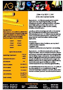
Silicone Coated Cable
by carny
Siwo - Kul B20 1.1kV Siwo - Kul B20 1.1kV Silicone...
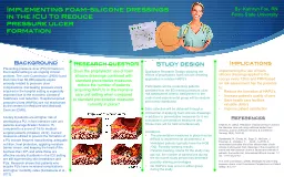
Implementing foam-silicone dressings in the ICU To Reduce
by fullyshro
pressure ulcer . formation. By: Kathryn Fox, RN. F...
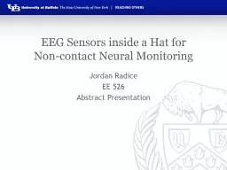
Dark Silicon Overview, Analysis and Future Work
by min-jolicoeur
Jordan . Radice. jordanra@buffalo.edu. Advanced ...
The Oasis Healthcare Centres – Excellence Medical Services for All
by medicalgulf
It is very significant to be the safe and healthy ...
Annaa Silicon Technology Private Limited
by test
VISION . To be a Customer focused Organization pr...
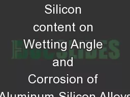
Effect of Silicon content on Wetting Angle and Corrosion of Aluminum-Silicon Alloys
by pamella-moone
Swaroop K. Behera. 1. , . Shvetashwa. Suri. 1. ...
Topological Light "Imaging topological edge states in Silicon photonics," M.
by faustina-dinatale
Hafezi. , S. Mittal, J. Fan, A. . Migdall. , J.M....
2 LIQUID SILICONE RUBBER
by olivia-moreira
. & . THERMOPLASTIC . ELASTOMERS. LSR’s...
Probabilistic Bug-Masking Analysis for Post-Silicon Tests i
by phoebe-click
Doowon Lee. *, Tom Kolan. †. , Arkadiy Morgensh...
Load More...