/
Circuits for sensors Circuits for sensors

Circuits for sensors - PowerPoint Presentation

sherrill-nordquist
sherrill-nordquist . @sherrill-nordquist
Follow
368 views
Uploaded On 2015-10-17

Circuits for sensors - PPT Presentation

Ideal OP Amps Basic OP Amp Circuit Blocks Analog Computation Nonlinear OP Amp Applications OP Amp Considerations Guarding Passive Filters Active Filters VCOVoltage Controlled Oscillator Chap 0 ID: 163977

amp chap voltage input chap amp input voltage gain pass high amplifier output frequency impedance differential filters filter passive

Share:

Link:

Embed:

Download Presentation from below link

Download Presentation The PPT/PDF document "Circuits for sensors" is the property of its rightful owner. Permission is granted to download and print the materials on this web site for personal, non-commercial use only, and to display it on your personal computer provided you do not modify the materials and that you retain all copyright notices contained in the materials. By downloading content from our website, you accept the terms of this agreement.


Presentation Transcript

Slide1

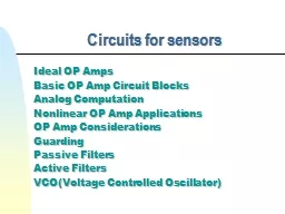
Circuits for sensors

Ideal OP Amps

Basic OP Amp Circuit Blocks

Analog Computation

Nonlinear OP Amp Applications

OP Amp Considerations

Guarding

Passive Filters

Active Filters

VCO(Voltage Controlled Oscillator)Slide2

Chap 0

2

Function of Amplifiers

Amplifiers provides

GAIN

Filtering, Signal processing, Correction for Nonlinearities

TemperaturePressureFlowMotion….

Sensor

Signal ConditioningCircuitry

DigitalComputerSlide3

Chap 0

3

Ideal OP Amps

Transfer Function = Output / Input

Voltage Amp TF (Gain):

Usually A

v  1OP Amp is preferredEasy to use in circuit designed compared to discrete Transistor circuitsSlide4

Chap 0

4

Ideal OP Amps (Cont.)

Assumptions

Open loop Gain = Infinity

Input Impedance Rd = Infinity

Output Impedance Ro = 0Bandwidth = InfinityInfinite Frequency Responsevo=0 when v1 = v2No Offset VoltageSlide5

Chap 0

5

Ideal OP Amps (Cont.)

Note

v

0

= A(v2 – v1)If v0 = , A =  (Typically 100,000)Then v2 – v1 = 0

 v2 = v1

Since v2 = v1 and Rd = We can neglect the current in RdRule 1

When the OP Amp is in linear range the two inputs are at the same voltageRule 2No Current flows into either terminal of the OP AmpSlide6

Chap 0

6

Basic OP Amp Circuit Blocks

Inverting Amplifier

Noninverting Amplifier

Unity-Gain AmplifierDifferential Amplifier

Instrumental AmplifierThe Electrocardiogram AmplifierSlide7

Chap 0

7

Inverting Amplifier

From Rule 1

v- = v+ = 0

From Rule 2 & KCL

ii + if = 0  ii = -if From Ohm’s lawii

= vi / Ri , , if = vo / R

f vi / Ri = - vo / Rf vo

/ vi = -Rf / RiInverting Amp Gain -Rf

/ Ri

Inverting Amp with Gain = - Rf / Ri

Virtual GroundSlide8

Chap 0

8

Inverting Amplifier (Cont.)

Linear Range

By Power Supply Voltage

Input Impedance

Low (Ri)Increasing Ri  Decreasing GainIncreasing Gain by increasing RfBut there is practical limit

SaturationSlide9

Chap 0

9

Noninverting Amplifiers

Noninverting Amp

Gain = (Rf + Ri) / Rf

By Rule 2

Vo = If  (Rf + Ri)Vi = If  RiVo = Vi  (Rf + Ri)/RiGain: Vo/Vi = 1 + Rf / RiGain

 1, AlwaysInput ImpedanceVery Large (Infinite)

By Rule 1

Vi Slide10

Chap 0

10

Unity-Gain Amplifier

Verify that the Gain of Unity-Gain Amp is 1

Vo = Vi

Applications

Buffer amplifierIsolate one circuit from the loading effects of a following stageImpedance converterData conversion System (ADC or DAC) where constant impedance or high impedance is requiredSlide11

Chap 0

11

Differential Amplifiers

Combination of Inverting and Noninverting Amp

Can reject 60Hz interference

Electrocardiogram amplifier

Differential

NoninvertingInstrumentationSlide12

Chap 0

12

Differential Amplifiers (Cont.)

Gain of Differential Amp

By Rule 2

V5 = I2 * R2

V2 = I2 * R1 + V5 = V5 * R1 /R2 + V5V5 = R2 * V2 / (R1 + R2)By Rule 1V1 = R1 * I1 + V5V5 = R2 * I1 + V6V6

= (V2 – V1) * R2 / R1Slide13

Chap 0

13

Differential Amplifiers (Cont.)

CMV (Common Mode Voltage)

If V1 = V2, then V6 = 0

CMG (Common Mode Gain) = 0

DG(Differential voltage Gain)If V1  V2, then V6 = (V2-V1)*(R2/R1)In practice, CMG  0CMRR (Common Mode Rejection Ratio)

Measure of the ability to reject CMVCMRR = DG / CMG

The Higher CMRR, the better qualityTypically, 100 ~ 10,00060Hz noise common to V1 and V2 can be rejectedSlide14

Chap 0

14

Instrumentation Amplifiers

One OP Amp Differential Amplifier

Input Impedance is not so High

Good for Low impedance source

Strain gage BridgeBad for High impedance sourceInstrumentation AmplifierDifferential Amp with High Input Impedance and Low Output ImpedanceTwo Noninvering Amp + One Differential AmpSlide15

Chap 0

15

Instrumentation Amplifiers (Cont.)

Instrumentation Amp = Noninverting Amp + Differential Amp

We have:

DG = (V1-V2) / (V3-V4)

= (2*R4 + R3) / R3V6 = (V3-V4)*DG*R2 / R1First Stage CMRRCMRR = DG / CMG = DGOverall CMG = 0High CMRR

High Input ImpedanceGain is adjustable by changing R3Slide16

Chap 0

16

The Electrocardiogram Amplifier

< 0.2

V

Gain = 40

Maximize CMRR

High Pass Filter

>0.05Hz

Low Pass Filter

< 100Hz

Gain = 32Slide17

Chap 0

17

Analog

Computation Circuit

Digital Signal Processing is preferred

Flexibility

Easy to ChangeElimination of hardwareHowever, Analog Signal ProcessingIs preferred when DSP consumes too much timeSlide18

Chap 0

18

Inverter and Scale Changer

Inverting Amp with Gain = - Rf / Ri

Inverter

Rf / Ri = 1

Inverter and Scale ChangerProper choice of Rf / RiApplicationUse of inverter to scale the output of DACSlide19

Chap 0

19

Adders (Summing Amplifiers)

Adder

Inverter with Several inputs

Vo = -Rf(V1/R1 + V2/R2 +… + Vn/Rn)

If = I1 + I2 + InI1 = V1/R1, …Vo = -If * RfRf determines overall GainRi determines weighting factor and input impedanceSlide20

Chap 0

20

Integrator

Drawbacks

Vo will reach saturation voltage, if Vi is left connected indefinitely

Integrator operates as an open-loop amplifier for DC inputsSlide21

Chap 0

21

Practical Integrator

Reset

S1 Closed, S0 Open

Inverter

C is initialized to VrIntegrate

S1 Open, S0 ClosedHoldS1 Open, S0 OpenKeeps Vo constant

Read and Process

Controlled By

Relay or

Solid State Switch or

Analog SwitchSlide22

Chap 0

22

Differentiators

Drawbacks

Instability at High frequencies

Practical Differentiator

To StableSlide23

Chap 0

23

Comparators

Compare Two Inputs

Vi > Vr

Vo = -Vs

Vi < VrVo = VsDrawbacksIf Vi = Vr + small noiseRapid fluctuation between  VsSlide24

Chap 0

24

Comparators with Hysteresis

Positive Feedback

Hysteresis loop

Can remove the effect of Small Noise

Reduce FluctuationSlide25

Chap 0

25

Rectifiers

Precision Half Wave Rectifier

Precision Full Wave Rectifier

LimitersSlide26

Chap 0

26

OP Amp Considerations

Effects of Nonlinear characteristics

Compensation

Undesirable Oscillation at High frequency

Add external Capacitance according to Spec sheetGBW (Gain Bandwidth Product)Gain  Bandwidth = Constant (Typically 1MHz)For Noninverting Amp: Bandwidth = GBW / GainInput Offset VoltagePractical OP AmpZero input Does NOT give Zero output

Input Offset VoltageApplied input voltage to obtain Zero outputNulling the offset VoltageAdding External Resister according to Spec sheetSlide27

Chap 0

27

OP Amp Considerations (Cont.)

Input Bias Current

Practical OP amp

Current flowing into the terminal is NOT Zero

To keep the input Tr of OP amp turned onCauses errors proportional to feedback network RTo minimize errorsfeedback R should be low (<10K)Slew RateMaximal rate of change of amplifier output voltageEx: Slew rate of 741 = 0.5 V /

sTime to output change from –5V to 5V = 20 sTo Minimize slew rate problem

Use OP amp with smaller external compensating CSlide28

Chap 0

28

OP Amp Considerations (Cont.)

Power Supply

Usually

15V

Linear Range 13VReducing power supply voltageResults reduced linear rangeDevice does not work < 4VDifferent OP AmpsBipolar Op Amps

Good input offset stabilityModerate input bias current and Input resistancesFET

Very Low input bias current and Very High Input resistancesPoor Input offset voltage stabilitySlide29

Chap 0

29

Guarding

Elimination of Surface Leakage Currents

Elimination of Common Mode Signals

Very important in practice

But skip in this courseSlide30

Chap 0

30

Passive Filters

Passive Circuits

Contains only passive elements

Registers, Capacitors and Inductors

ExamplesBridge CircuitVoltage DividerFiltersFiltersEliminate unwanted signal from the loopLow Pass, High Pass, Band Pass, Notch, …Slide31

Chap 0

31

Passive first-order Low pass Filter

Pass desired Audio signal and reject undesired RF

Order of Filter

Number of C and L

Plot Magnitude and Phase plot (Bode plot)Meaning of CSlide32

Chap 0

32

Passive first-order High pass Filter

Pass desired High frequency signal and reject undesired low frequency signal

Plot Magnitude and Phase plot (Bode plot)

Meaning of 

CSlide33

Chap 0

33

Passive second-order Low pass Filter

To increase the attenuation of transfer function

Order of Filter

Number of C and L

Meaning of Quality factorSlide34

Chap 0

34

Passive second-order High pass Filter

To increase the attenuation of transfer function

Order of Filter

Number of C and LSlide35

Chap 0

35

Active First-order Low Pass Filter

Inverting Amp + Feedback Capacitor

Identical frequency response with Passive filter

Very Low Output impedance

Negligible Loading EffectSlide36

Chap 0

36

Active First-order High Pass Filter

Inverting Amp + Input Capacitor

Identical frequency response with Passive filter

Very Low Output impedance

Negligible Loading EffectSlide37

Chap 0

37

Active High-order Filters

Low Pass Filters

High Pass FiltersSlide38

Chap 0

38

Bandpass and Band-reject Filters

Butterworth Filters

Maximally Flat Magnitude response in pass band

High Attenuation Rate

Chebyshev FiltersMaximum Attenuation RateRipple in pass bandBessel FiltersMaximally flat time delay in response to step inputAttenuation Rate is very gradualSlide39

Chap 0

39

Filter Design Table

C when

0

= R0 = 1Slide40

Chap 0

40

Filter Design Example

Low pass five-pole Butterworth filter with a corner frequency of 200Hz and input resistance of 50K

Economic Solution = 3

rd order + 2nd orderDesired R and C ?C1A = (0 R0

C0 ) / ( R) = 1x1x

1.753 / 2x200x50K = 27.9 nFC2A = 21.6 nF, C3A = 6.7 nF, C

1B = 51.5 nF, C2B = 4.9 nF Slide41

Chap 0

41

VCO(Voltage Controlled Oscillator)

VCO = Voltage to Frequency(V/F) Converter

VCO converts an input voltage to a series of output digital pulses

whose frequency is proportional to the input voltage

ApplicationsADCDigital TransmissionTelemetryDigital VoltmeterSlide42

Chap 0

42

VCO (Cont.)

Module form

Better linearity, Lower Gain drift, Higher full-scale frequencies than IC

Monolithic IC form

Less expensive, Small sizeLower drift, Better flexibility of frequency rangeExamplesLM331Low cost VCO from National SemiconductorMaximum nonlinearity 0.01% over 1 ~ 100KHzCD4046BPLL contains VCO

Maximum nonlinearity 1.0% over 1 ~ 400MHzSlide43

Chap 0

43

PLL(Phase Locked Loop)

VCO is commonly used in PLL

Applications

Communications

RadarTime and frequency controlInstrumentation systemControl loopGoalMinimize z(t)

 s(t) = r(t)Change r(t) until z(t)=0s(t) can be obtained By reading r(t)Slide44

Chap 0

44

VCO Interfacing

Output of VCO

Digital pulses whose frequency is proportional to input voltage

#

of pulse / DurationDurationControlled by Sampling Gate# of PulseCounted in CounterSlide45

Chap 0

45

Divider Circuit

Convert Register Variations to Voltage Variations

Output Voltage

Vo = {R2 / (R1 + R2)} Vs

R1

R2

Vs

VoSlide46

Chap 0

46

Divider Circuit: Drawbacks

Vo is not linearly changed

Ex: Vs = 5V, R1 = 1K

, R2 = 0 ~ 1K(Sensor)

Output Impedance(R1 || R2) is not so High

Large Power Consumption

R2

Vo

1

K

500

Vs/2

Vs/3Slide47

Chap 0

47

Divider Circuit: Example

R1 = 10K

, R2 = (4K ~ 12K), Vs = 5V

Maximum Vo = 5 {12 / (10+12)} = 2.73V

Minimum Vo = 5 { 4 / (10 + 4)} = 1.43VMaximum Z = (10K || 12K) = 120/22 KMinimum Z = (10K || 4K) = 40/14 KMaximum Power = (Vo)2/R2 = (2.73)2

/12K = 0.62mWMinimum Power = (1.43)2/4K = 0.51mW