/
An Analog Method to Study the Average Memory Access Time in a Computer System Yash Pal An Analog Method to Study the Average Memory Access Time in a Computer System Yash Pal

An Analog Method to Study the Average Memory Access Time in a Computer System Yash Pal - PDF document

stefany-barnette
stefany-barnette . @stefany-barnette
Follow
553 views
Uploaded On 2014-12-11

An Analog Method to Study the Average Memory Access Time in a Computer System Yash Pal - PPT Presentation

g summation integration differentiation scaling etc We can calculate the average access time with this analog method with high speed and high degree of versatality This paper evaluates the three most common parameters of the Memory system ie access t ID: 21986

summation integration differentiation scaling

Share:

Link:

Embed:

Download Presentation from below link

Download Pdf The PPT/PDF document "An Analog Method to Study the Average Me..." is the property of its rightful owner. Permission is granted to download and print the materials on this web site for personal, non-commercial use only, and to display it on your personal computer provided you do not modify the materials and that you retain all copyright notices contained in the materials. By downloading content from our website, you accept the terms of this agreement.


Presentation Transcript

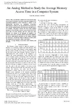
An Analog Method to Study the Average Memory Access Time in a Computer System Yash Pal, Member, IAENGAbstract -This is an attempt to simulate the concept of average access time of the memory system by using some analog devices (operational amplifiers) whose behaviour is similar to the mathematical operations e.g. summation, integration, differentiation, scaling etc. We can calculate the average access time with this analog method with high speed and high degree of versatality. This paper evaluates the three most common parameters of the Memory system i.e access time of the RAM, access time of Cache memory and the Cache hit ratio. Basically, the voltages in the high-gain dc amplifiers are equated to these three variables and the operational amplifiers can do the mathematical operations on the voltages, athough the accuracy of measuring voltage is limited to certain point. The simulation has been done using CircuitMaker. Keywords -Average Memory Access time, Cache Memory and OPAMPs INTRODUCTION The Memory system consists of physical memory i.e. Random Access Memory (RAM) and Cache Memory. The average access time of the Memory system depends upon the access time of RAM, Access time of cache memory and the Hit Ratio of the Cache Memory. The basic reason for implementing the cache memory in the computer is to improve the system performance. Every time the CPU accesses memory system, it checks the cache. If the required Physical Address 0 1 2 3 4 5 6 7 Data 20 40 10 20 30 30 80 40 Physical Address 8 9 10 11 12 13 14 15 Data 20 10 90 20 10 12 14 20 Since the Associative Mapping[9] of Cache memory contains the complete physical address and data at that address in single location of cache, the Cache activity can be shown as in Table where the first row in the table depicts the physical addresses referred by the CPU and the contents of columns below these referred addresses tell the contents of cache locations 0 to 3 after the address is referred. The last row specifies that Hit operation has happened or not. TABLE II CONTENTS OF ASSOCIATIVE CACHE MEMORY Physical Address es 0 1 2 0 10 9 2 6 Cache memory addresses 0 20 20 20 20 20 10 10 10 1 40 40 40 40 40 40 80 2 10 10 10 10 10 10 3 90 90 90 90 ISBN: 978-988-19252-8-2 ISSN: 2078-0958 (Print); ISSN: 2078-0966 (Online) WCE 2013 Hit NO NO NO YES NO NO YES NO So, the hit ratio of Associative Cache = (Number of hits)/(Total Number of addresses referred) =2/8 = 0.25. Thus, the average memory access time = 0.25* + 0.75*700 = 550ns. The Direct-mapped cache memory contains the tag and data in its single location which is determined from the index part of the physical address being referred. This means that two physical locations with different tags and same index cannot be stored in the cache memory at the same time. In the given case, the physical address is 4-bits Proceedings of the World Congress on Engineering 2013 Vol II, WCE 2013, July 3 - 5, 2013, London, U.K. long. The cache is having only four locations. So, the index part is 2-bits long(because log4 = 2). So the data value 90 having physical location 10=(1010) address ending with the bits 10 will be stored along with the tag part (10)only in cache location (10). Thus as per the Table III, The hit ratio of Direct-mapped cache memory = 1/8 = 0.125 The average memory access time = 0.125*100 + 0.775*700 = 543.75. TABLE CONTENTS OF DIRECT CACHE MEMORY Similarly, in Two-way set associative cache two sets of tag and data can be stored in single location of cache. In this two different physical addresses with different tags and same index can be stored in the cache. Thus, as per the Table IV, The hit ratio of Two-way set associative cache = 2/8 = 0.25 and The average memory access time = 0.25*100 + 0.75*700 = 550ns TABLE CONTENTS OF SET-ASSOCIATIVE CACHE MEMORY Physical Addresses 0 1 2 0 10 9 2 6 Cache Memory addresses 0 20 20 20 90 90 90 90 0 10 10 10 10 10 80 1 40 40 40 40 40 40 40 1 10 10 10 Hit NO NO NO YES NO NO YES NO OPERATIONAL AMPLIFIEAn Operational amplifier (OPAMP as generally called) the basic element of an analog circuit design. is a high gain amplifier[4] which has so many applications. The amplifiers can be specified in the terms of gain, input impedance, output impedance, bandwidth, and offset characterstics. These are normally used in amplifier and alog signal processing circuits in frequency band 0 KHz to 100 KHzKHz]. The OPAMPs which were first developed were vacuum tube circuits used in analog computers. Now OPAMPs are fabricated as ICs (Integrated chips) which are completely different from the earliest OPAMPs. The Ideal OPAMP is a three-terminal circuit element that is modeled as voltage-controlled voltage source[7]. The OPAMP electronic circuit diagram and circuit symbol (or analog diagram) can be given as in Fig. 1 and Fig2. Its output voltage is a gain multiplied by its input voltage. The input voltage is the difference voltage between the two input terminals. The output voltage is measured w.r.t. the circuit ground node. Fig. 1. Ideal OpampFig. 2Ideal Opamp Circuit SymbolThe equation for output voltage can be given as - V), where Ais the voltage gain. 2 is the voltage at non-inverting input and V is the voltage at inverting input. The input terminals have four characterstics, which are There is no current in each input lead, which means that resistance in both input terminals is infinite. The output voltage does not depend upon output current, which implies that voltage gain is independent of output current. The voltage gain A doesnot depend on frequency, which infers bandwidth is infinite. iv)The voltage gain Ais very large reaching infinity in limit, which implies that the difference voltage between two input terminals must approach zero if the output voltage is finite. Inverting Operational Amplifier The voltage gain is negative, it is called as an inverting operational amplifier[6]. It implies that if the input voltage is positive, the output voltage will be negative and vice-versa. The input voltage is applied through the resistor R to inverting input terminal as shown in Fig. 3. The Resistor Ris the feedback resistor which connects from the output to the inverting input. The voltage gain in the inverting OPAMP is given by -R)*V (1.2) Summing Operational Amplifier The summer circuit actually behaves like the mathematical sum operation[8]. The n-input summer circuit can be shown as Fig. According to the Kirchhoff’s current law at the junction B, the sum of all currents passing through the junction is zero.i.e + I+........I + If I= 0 + I + I= IB which can be further written as V)/R + V)/R+................+ V)/R+ V) = VAs Vbe given as Vg -A-V), and also V, so we get Phys ical Addresses 0 1 2 0 10 9 2 6 Cache memory addresses 0 20 20 20 20 20 20 20 20 1 40 40 40 40 40 10 10 2 10 10 90 90 10 80 3 Hit NO NO NO YES NO NO NO NO R out V 0 V g = - A v (V 1 - V 2 ) R in V g + - - V 1 V 2 - + V 0 V 1 V 2 + V+..................+ V+ V/R-V (1.3) where 1/Rp = 1/R+ 1/R+..............1/R+ 1/RFig. 3Inverting OpampThis operational amplifier has a high voltage gain, so we can consider A to be infinite. Then the equation (1.3) can be rewritten as 0 (1.4) here α= Rand i = 1,2,3,..............n. Fig. 4Summer Circuit The example of summation of three voltages is shown in Fig. 5. In this example three resistances (RI,R2,R3) of 10 kΩ each and R= 100kΩ has been used.Thus,α= α= α3 =10.So the summer in the Fig. 5 implements the equation (1.4) as, = -2 and the analog diagram can be given as Fig. 5. Summer Circuit Symbol Multiplication of Reference voltage by a constant To implement this the potentiometer is used which is basically a voltage divider and the input voltage is fractioned by a value determined by the amount of resistance choosen. =KV. 6 and Fig7 shows the analog diagram and electrical circuit. ultiplier Circuit Fig. 7Multiplier Circuit Symbol THEORETICAL DEVELOPEMENT To simulate the mathematical equation (1.1), we can use an analog method by the use of operational amplifiers. An analog method can be applied to find solutions of a number of diferential equations, linear equations etc[3]The system which is to be simulated is first modelled by a mathematical equation and the analog diagram for the system (in this case the Memory system of any computer) can be given as in FigFig. 8. Analog Diagram for (1.1). The electronic circuit diagram for the mathematical equation (1.1) can be given as in Fig.9. There are six Ideal OPAMPs (U1, U2, U3, U4, U5, U6) which have been used for implementation of (1.1). We have implemented six multimeters so that output of each OPAMP can be watched. The Vs1 and Vs2 represent the access times of the Cache Memory, t and access of the RAM, tm respectively. 1 1 - Summer & Inverter Inverter Summer & Inverter 1 - + h t m t a 1 t c t m - + h + 1 K V i V 0 V i V 0 B 1 R o ut R n V 0 R f V 1 V n I f R in V g R 1 I 1 I n + - - + - 10 V 1 V 2 V 3 V 0 10 10 - + R out R f - - + - I f R in V g + - - I 1 B 1 R 1 V 0 V 1 Fig. 9.Simulation of Equation (1.1) using Circuit Maker. The above instance of the circuit shows Vs1 = 100V that is =100ns and Vs2 = 700V that is, t=700ns(The access times are normally evaluated in the units of nanoseconds, we can represent the time unit of 1ns by 1V of the voltage supplies used in the Fig. 9 The hit ratio in the circuit is represented by the fractions as below h= R4/R6=R9/R8 and it can be varied by changing the values of the resistors R4,R6 and R9,R8 such that the ratios of these respectively should be same. In the given circuit, h=0.9, as R4=0.9kΩ and R6=10kΩ.We just see the working of each OPAMP one by one. The first ideal OPAMP U2 outputs the fraction h of Voltage Vs1 but in negative. We can consider it like multiplication of Vs1 with the constant R4/R6, that is, h. Thus, the output represents h*t. The second ideal OPAMP U5 outputs the negative of input Voltage. Thus, the output represents h*t. The third ideal OPAMP U3 is a summer and inverter. It first sums the h fraction of Vs1 with the Vs2 and gives the output in negative voltage. Thus the output represents the lue (h*t + t) . The fourth ideal OPAMP U4 outputs the fraction h of Voltage Vs2 but in negative. We can consider it like multiplication of Vs2 with the constant R9/R8, that is, h. Thus the output represents the the val h*t. The fifth ideal OPAMP U1 outputs the negative of the input Voltage. Thus, the output represents h*t. The sixth ideal OPAMP U6 is a summer and inverter. This OPAMP sums the output of ideal OPAMP U3 and U1 and gives the output in negative. Thus the output represents the value (- (h*t+ t) + ) which can be rewritten as h*tc + tm -h*tm = h*t+ -h)*t. Thus the output of OPAMP U6 represents t. The circuit was used to study the change in the average memory access time, t, for different values of hit ratio with = 100ns and tm = 700ns. The values for t shown by the multimeter attached at the output of U6 OPAMP for different values of h = R4/R6 = R9/R8 are given in the Table V. TABLE V VALUES OF t OBTAINED WITH DIFFERENT h AND CONSTAN =100ns AND tm =700ns. h t a in ns 0 700 0.1 640 0.2 580 0.3 520 0.4 460 0.5 400 0.6 340 0.7 280 0.8 220 0.9 160 1 100 IV.CONCLUSION The possible drawback of any electronic analog computer simulation is so many assumptions in deriving the lationships for operational amplifiers[5]. It has the difficulty to carry accuracy of measuring a voltage beyond a certain limit. We also have to dedicate an analog computer to one problem. Although there is widespread availability of Digital Computers, many users prefer to use analog computers. The analog representation of a system is often more natural in the sense that it directly reflects the structure of the system ultimately simplifying the DC V 90.00 V U5 IDEAL U2 IDEAL + - Vs1 100V DC V -90.00 V DC V 630.0 V U1 IDEAL + - Vs2 700V DC V 160.0 V U6 IDEAL U4 IDEAL DC V -630.0 V DC V -790.0 V U3 IDEAL R13 1k R10 1k R4 .9k R6 1k R3 1k R1 1k R14 1k R12 1k R11 1k R8 1k R9 .9k R7 1k R5 1k R2 1k implementation of simulation and understanding of the result The use of analog computers is extended by developments in solid-logic electronic devices[6]Under certain conditions, an analog computer is faster than a digital computer, because it can solve many mathematical equations in a true simultaneous manner. REFERENCES [1]John D. CarpinelliComputer Systems Organization and Architecture, Seventh Impression, Dorling Kindersley (India) Pvt. Ltd., licensees of Pearson Education in South Asia.publishing,pp.391-395. [2]M.Morris Mano, Computer System Architecture, Third Edition, Pearson Printice Hall, India, pp.449. [3]Murray, Francis J., Mathematical Machines, vol.2 Analog Devices, New York: Columbia Press, 1961. [4]Granino Arthur Korn and Theresa M. Korn, Electronic Analog and Hybrid Computers, New York: McGraw-Hill Book Company, 1972. [5]Geoffrey Gordon, System Simulation, Second Edition, Eastern Economy Edition, PHI company, pp. 62-66. ] Robert Paz,Analog Computer Programming. ] Walt Kester, Editor,High Speed Design Techniques,Analog Devices,1996, ISBN0-916550--6. [8]Sergio Franco, Design with Operational Amplifiers and Analog Integrated Circuits, Second Edition, McGrawHill, 1998, pp.17-50. ] K.Hwang, Faye A Briggs, Computer Architecture and Parallel Processing, McGrawHillCompany, 1984, pp102-108. Proceedings of the World Congress on Engineering 2013 Vol II, WCE 2013, July 3 - 5, 2013, London, U.K.