PPT-Issue with DCLK divider=1 for CLKout0 and 1 (FPGA clock and SYSREF)
Author : victoria | Published Date : 2023-11-11
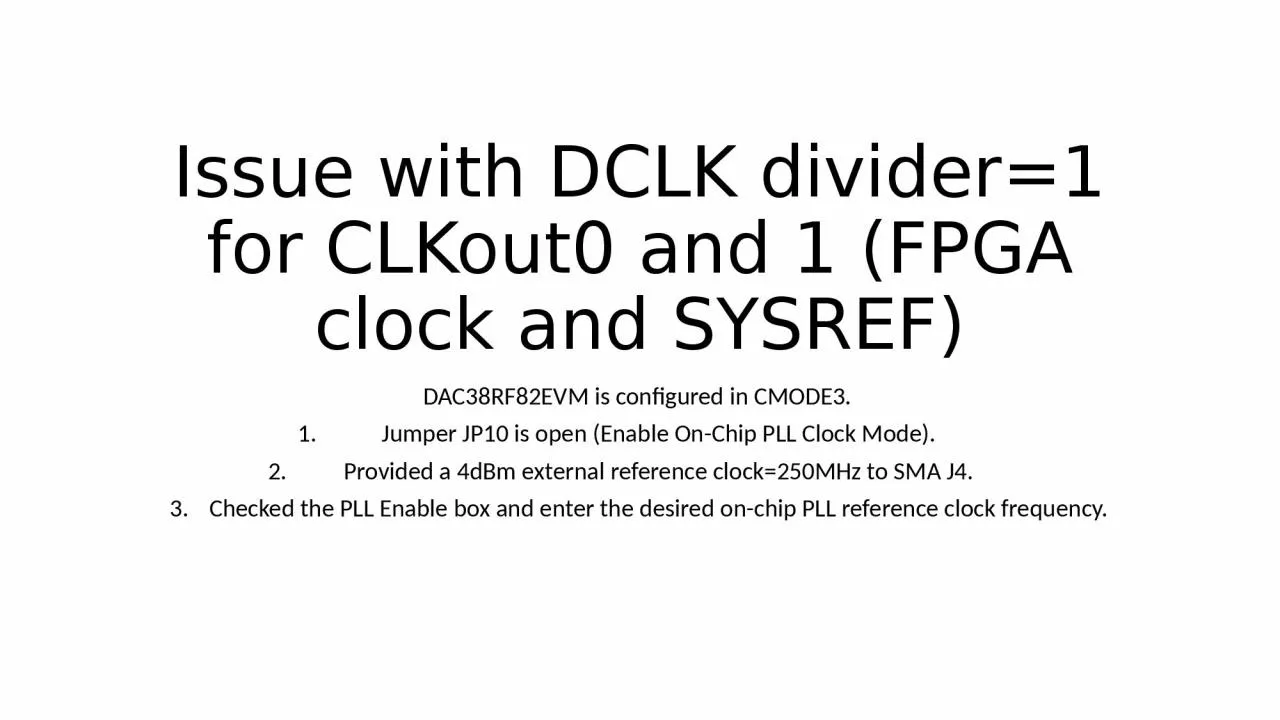
DAC38RF82EVM is configured in CMODE3 Jumper JP10 is open Enable OnChip PLL Clock Mode Provided a 4dBm external reference clock250MHz to SMA J4 Checked the PLL Enable
Presentation Embed Code
Download Presentation
Download Presentation The PPT/PDF document "Issue with DCLK divider=1 for CLKout0 an..." is the property of its rightful owner. Permission is granted to download and print the materials on this website for personal, non-commercial use only, and to display it on your personal computer provided you do not modify the materials and that you retain all copyright notices contained in the materials. By downloading content from our website, you accept the terms of this agreement.
Issue with DCLK divider=1 for CLKout0 and 1 (FPGA clock and SYSREF): Transcript
Download Rules Of Document
"Issue with DCLK divider=1 for CLKout0 and 1 (FPGA clock and SYSREF)"The content belongs to its owner. You may download and print it for personal use, without modification, and keep all copyright notices. By downloading, you agree to these terms.
Related Documents