Bipolar Junction Transistors(BJT) Chapter3 The BJT is constructed with three doped semiconductor regions separated by two pn junctions, as shown in the epitaxial planar structure in Figure 3.1(a). The three regions are called emitter (E),
"Bipolar Junction Transistors(BJT) Chapter#3 The" is the property of its rightful owner. Permission is granted to
download and print the materials on this website for personal, non-commercial use only, and to display it
on your personal computer provided you do not modify the materials and that you retain all copyright
notices contained in the materials. By downloading content from our website, you accept the terms of this
agreement.
Presentation Transcript
01
Bipolar Junction Transistors(BJT) Chapter#3<br>
02
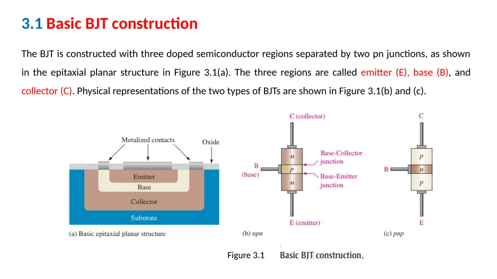
The BJT is constructed with three doped semiconductor regions separated by two pn junctions, as shown in the epitaxial planar structure in Figure 3.1(a). The three regions are called emitter (E), base (B), and collector (C). Physical representations of the two types of BJTs are shown in Figure 3.1(b) and (c). Figure 3.1 3.1 Basic BJT construction<br>
03
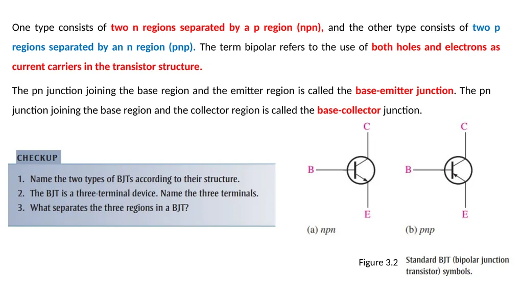
One type consists of two n regions separated by a p region (npn), and the other type consists of two p regions separated by an n region (pnp). The term bipolar refers to the use of both holes and electrons as current carriers in the transistor structure. The pn junction joining the base region and the emitter region is called the base-emitter junction. The pn junction joining the base region and the collector region is called the base-collector junction. Figure 3.2<br>
04
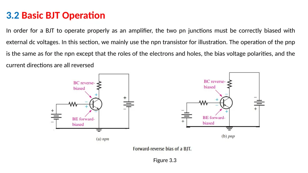
3.2 Basic BJT Operation In order for a BJT to operate properly as an amplifier, the two pn junctions must be correctly biased with external dc voltages. In this section, we mainly use the npn transistor for illustration. The operation of the pnp is the same as for the npn except that the roles of the electrons and holes, the bias voltage polarities, and the current directions are all reversed Figure 3.3<br>
05
The heavily doped n-type emitter (E) region has a very high density of conduction-band (free) electrons. These free electrons easily diffuse through the forward-based BE junction into the lightly doped and very thin p-type base region. The base (B) has a low density of holes, which are the majority carriers. A small percentage of the total number of free electrons injected into the base region recombine with holes and move as valence electrons through the base region and into the emitter region as hole current. Figure 3.4 Most of the free electrons that have entered the base do not recombine with holes because the base is very thin. As the free electrons move toward the reverse-biased BC junction, they are swept across into the collector region by the attraction of the positive collector supply voltage. The free electrons move through the collector region, into the external circuit, and then return into the emitter region along with the base current, as indicated.<br>
06
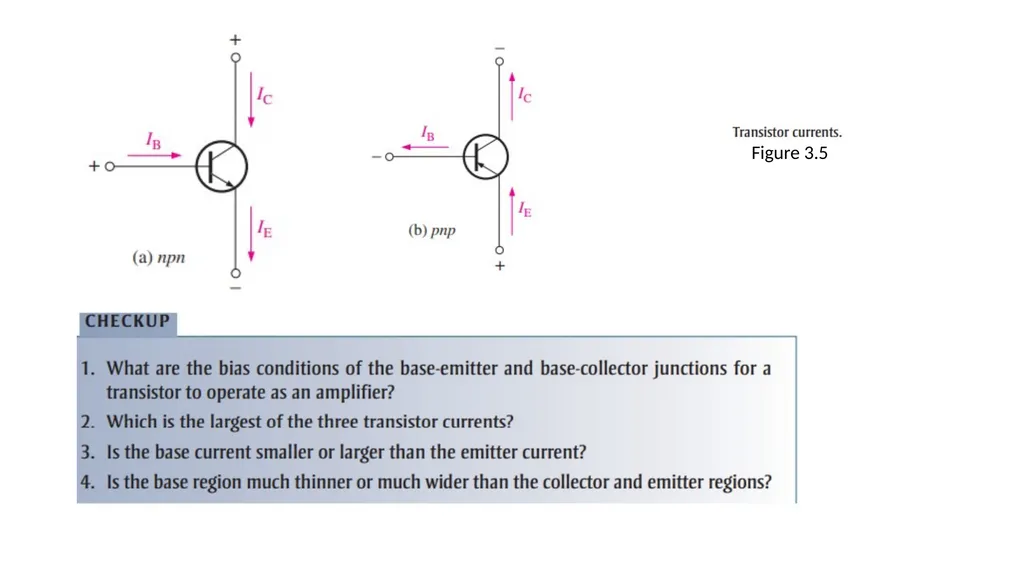
Figure 3.5<br>
07
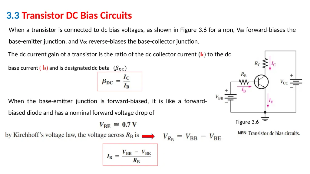
3.3 Transistor DC Bias Circuits When a transistor is connected to dc bias voltages, as shown in Figure 3.6 for a npn, VBB forward-biases the base-emitter junction, and VCC reverse-biases the base-collector junction. Figure 3.6 When the base-emitter junction is forward-biased, it is like a forward-biased diode and has a nominal forward voltage drop of<br>
08
The voltage at the collector with respect to the grounded emitter is<br>
09
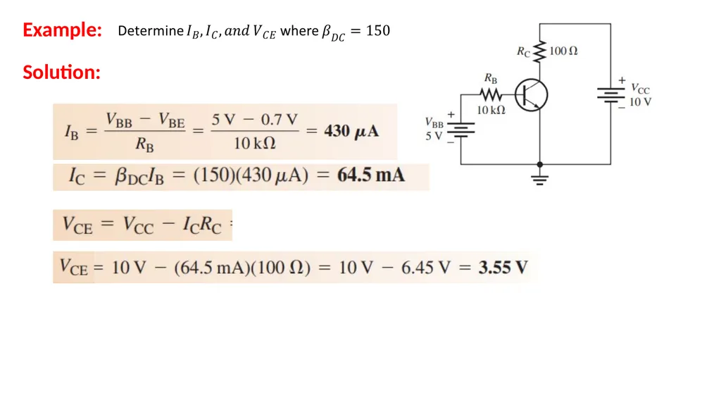
Example: Solution:<br>
10
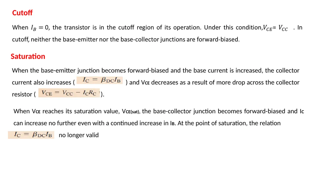
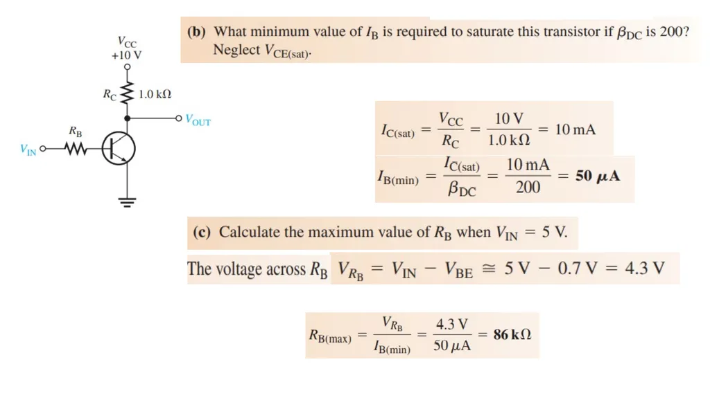
Cutoff Saturation<br>
11
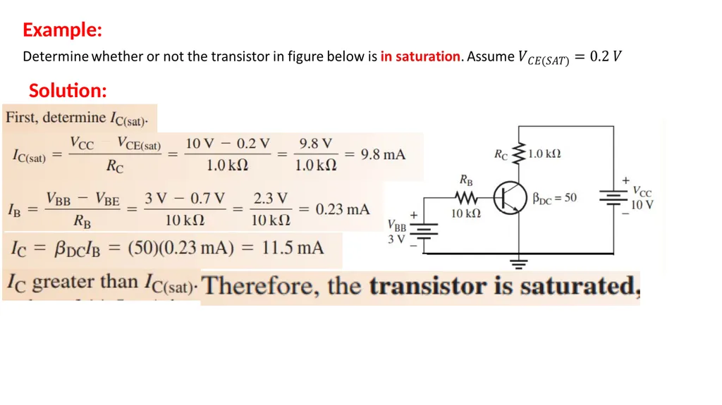
Example: Solution:<br>
12
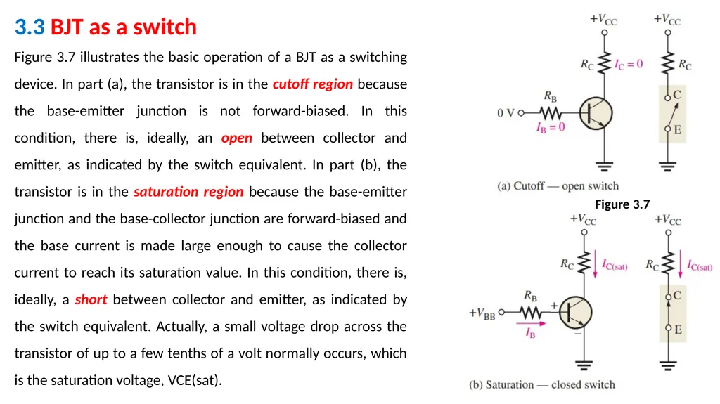
3.3 BJT as a switch Figure 3.7 illustrates the basic operation of a BJT as a switching device. In part (a), the transistor is in the cutoff region because the base-emitter junction is not forward-biased. In this condition, there is, ideally, an open between collector and emitter, as indicated by the switch equivalent. In part (b), the transistor is in the saturation region because the base-emitter junction and the base-collector junction are forward-biased and the base current is made large enough to cause the collector current to reach its saturation value. In this condition, there is, ideally, a short between collector and emitter, as indicated by the switch equivalent. Actually, a small voltage drop across the transistor of up to a few tenths of a volt normally occurs, which is the saturation voltage, VCE(sat). Figure 3.7<br>
13
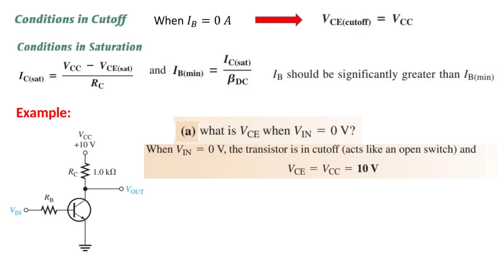
Example:<br>
14
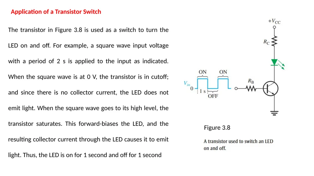
Application of a Transistor Switch The transistor in Figure 3.8 is used as a switch to turn the LED on and off. For example, a square wave input voltage with a period of 2 s is applied to the input as indicated. When the square wave is at 0 V, the transistor is in cutoff; and since there is no collector current, the LED does not emit light. When the square wave goes to its high level, the transistor saturates. This forward-biases the LED, and the resulting collector current through the LED causes it to emit light. Thus, the LED is on for 1 second and off for 1 second Figure 3.8<br>
15
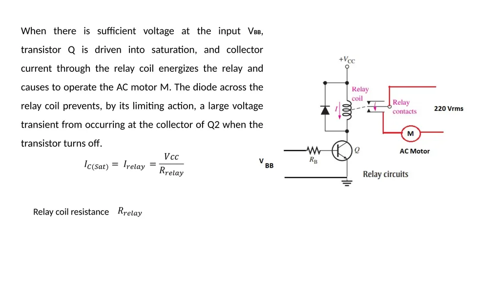
When there is sufficient voltage at the input VBB, transistor Q is driven into saturation, and collector current through the relay coil energizes the relay and causes to operate the AC motor M. The diode across the relay coil prevents, by its limiting action, a large voltage transient from occurring at the collector of Q2 when the transistor turns off. Relay coil resistance<br>