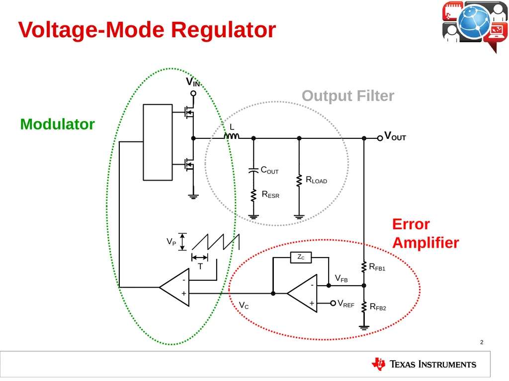
Buck Regulator Architectures 4.6 Voltage Mode Buck Regulators Voltage-Mode Regulator 2 Output Filter Error Amplifier Modulator Advantages and Disadvantages Advantages Stable modulationless sensitive to noise Single feedback path Can work
"Buck Regulator Architectures 4.6 Voltage Mode Buck" is the property of its rightful owner. Permission is granted to
download and print the materials on this website for personal, non-commercial use only, and to display it
on your personal computer provided you do not modify the materials and that you retain all copyright
notices contained in the materials. By downloading content from our website, you accept the terms of this
agreement.
Presentation Transcript
01
Buck Regulator Architectures 4.6 Voltage Mode Buck Regulators<br>
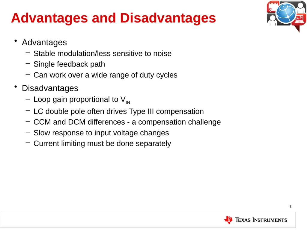
Advantages and Disadvantages Advantages
Stable modulation/less sensitive to noise
Single feedback path
Can work over a wide range of duty cycles
Disadvantages
Loop gain proportional to VIN
LC double pole often drives Type III compensation
CCM and DCM differences - a compensation challenge
Slow response to input voltage changes
Current limiting must be done separately 3<br>
04
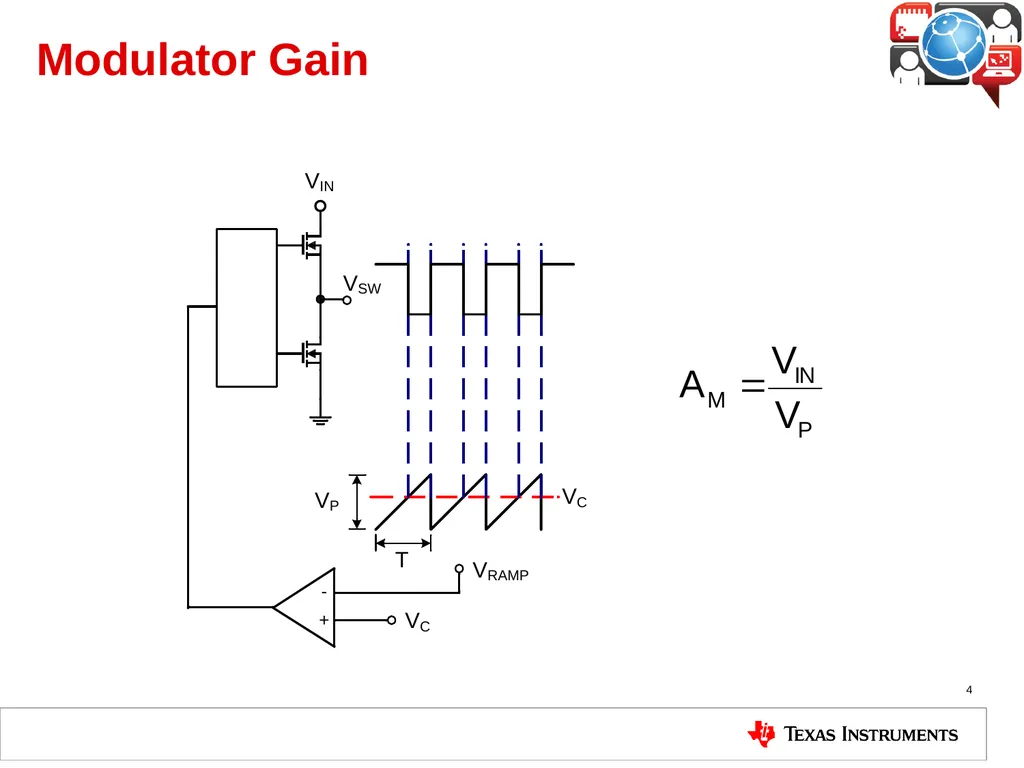
Modulator Gain 4<br>
05
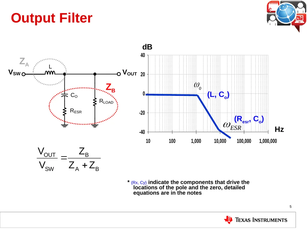
Output Filter 5 ZA ZB * (Rx, Cy) indicate the components that drive the locations of the pole and the zero, detailed equations are in the notes dB Hz (L, Co) (Resr, Co)<br>
06
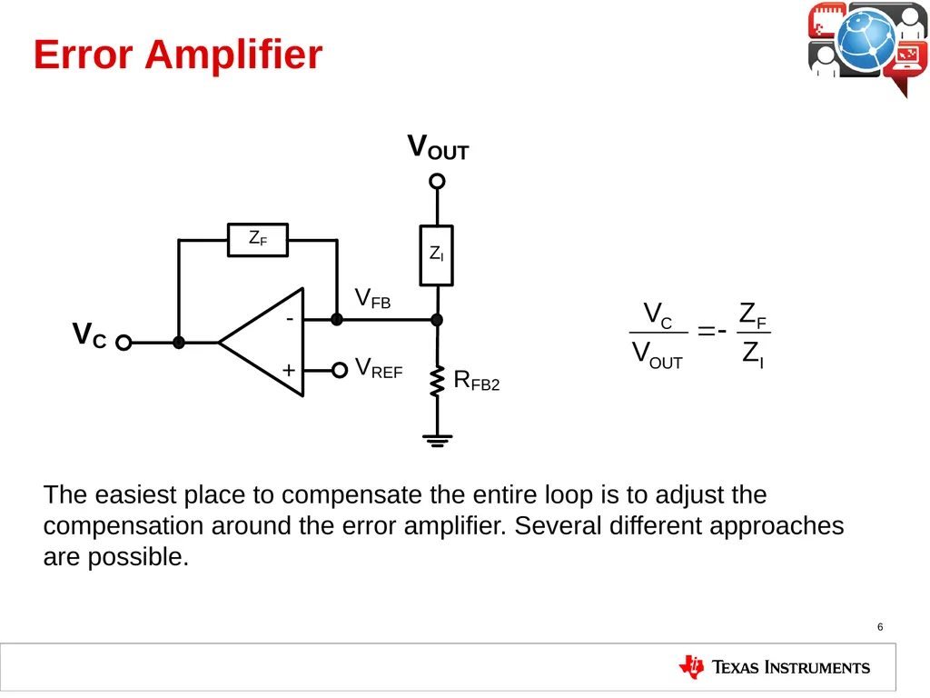
Error Amplifier The easiest place to compensate the entire loop is to adjust the compensation around the error amplifier. Several different approaches are possible. 6<br>
07
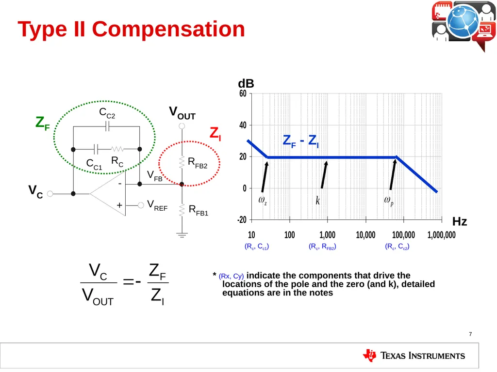
Type II Compensation 7 ZI * (Rx, Cy) indicate the components that drive the locations of the pole and the zero (and k), detailed equations are in the notes ZF - ZI dB Hz (Rc, Cc1) (Rc, Cc2) (Rc, RFB2)<br>
08
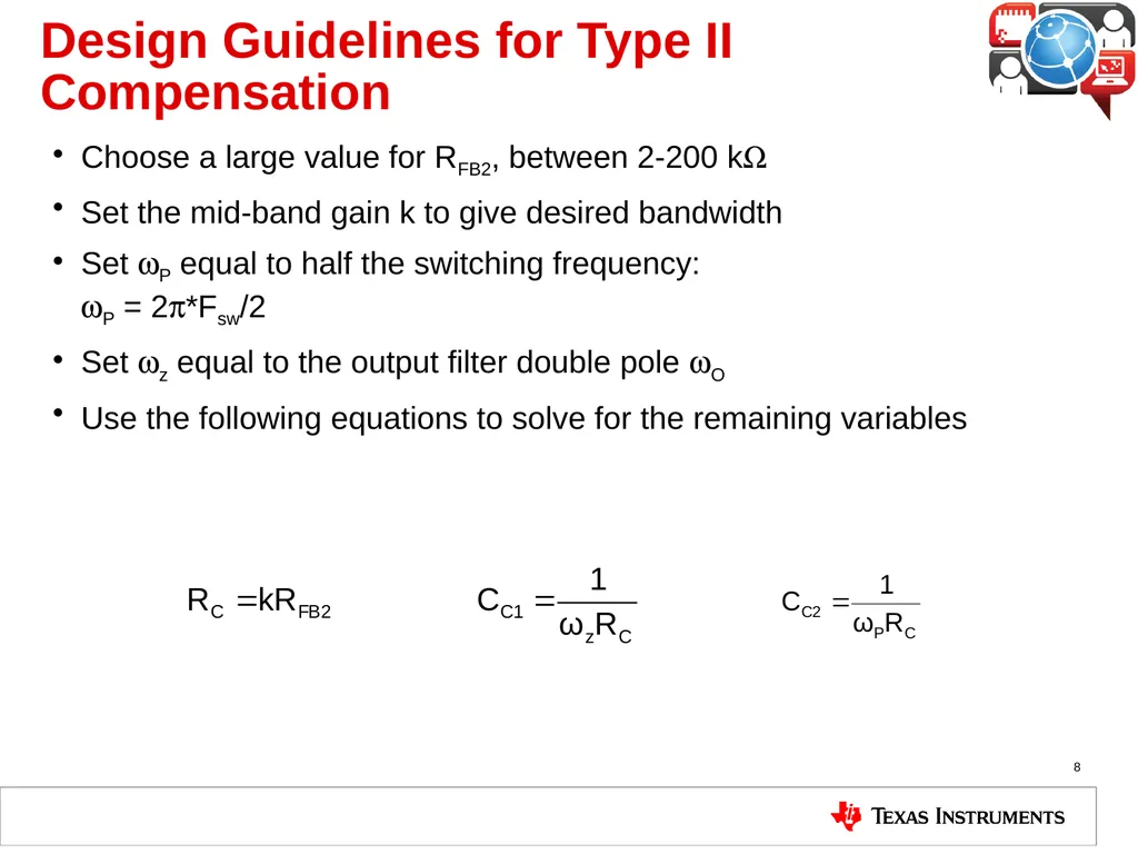
Design Guidelines for Type II Compensation Choose a large value for RFB2, between 2-200 kW
Set the mid-band gain k to give desired bandwidth
Set wP equal to half the switching frequency: wP = 2p*Fsw/2
Set wz equal to the output filter double pole wO
Use the following equations to solve for the remaining variables 8<br>
09
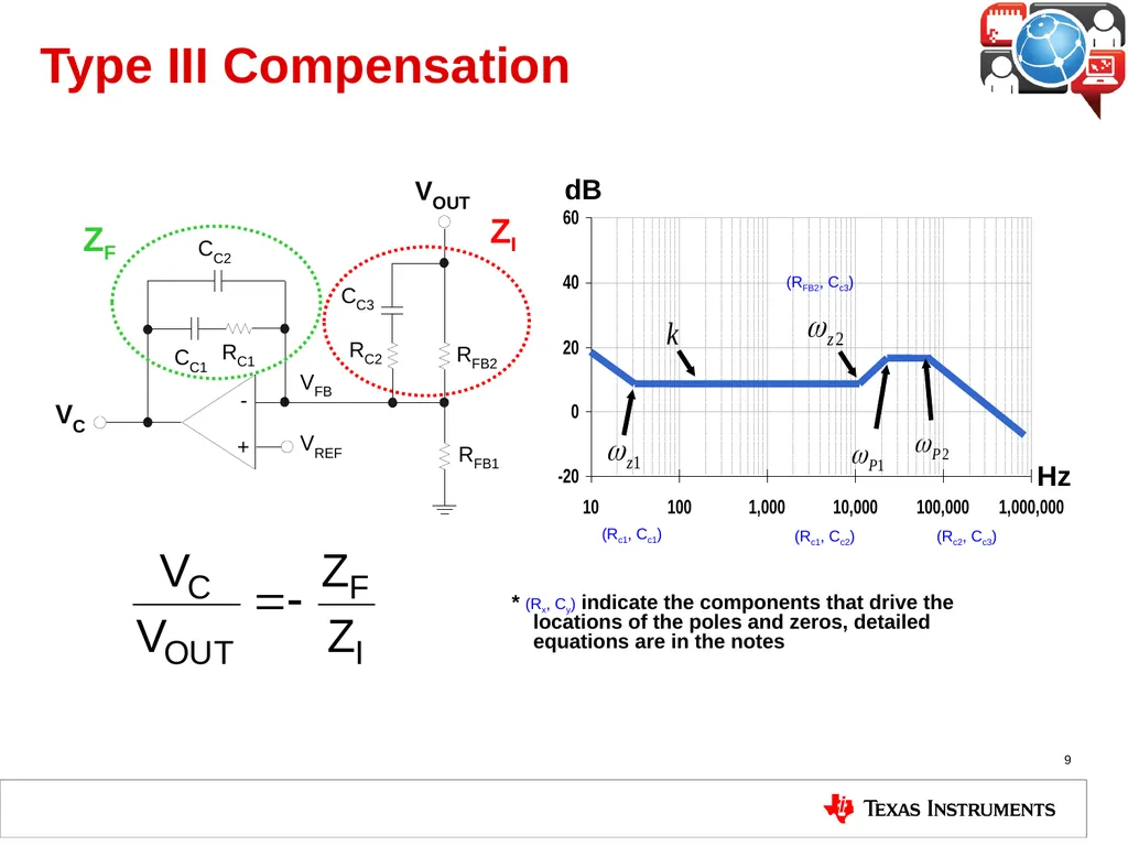
Type III Compensation 9 ZF ZI * (Rx, Cy) indicate the components that drive the locations of the poles and zeros, detailed equations are in the notes dB Hz (Rc1, Cc1) (RFB2, Cc3) (Rc1, Cc2) (Rc2, Cc3)<br>
10
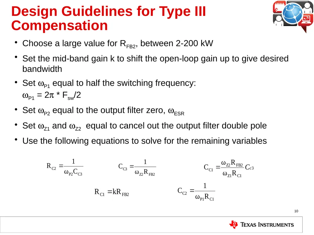
Design Guidelines for Type III Compensation Choose a large value for RFB2, between 2-200 kW
Set the mid-band gain k to shift the open-loop gain up to give desired bandwidth
Set wP1 equal to half the switching frequency: wP1 = 2p * Fsw/2
Set wP2 equal to the output filter zero, wESR
Set wZ1 and wZ2 equal to cancel out the output filter double pole
Use the following equations to solve for the remaining variables 10<br>
11
Internal Type III Voltage Mode Compensation (LM367x) 11 Typical Application Circuit Internal Block Diagram<br>
12
Internal Type III Voltage Mode Compensation (LM285x) 12 Typical Application Circuit Internal Block Diagram<br>