04
Memory Subsystem Power Memory subsystem power a significant portion<br>
05
Memory Subsystem Power Memory subsystem power a significant portion
DRAM<br>
06
Memory Subsystem Power Memory subsystem power a significant portion
DRAM, Buffers<br>
07
Memory Subsystem Power Memory subsystem power a significant portion
DRAM, Buffers, Caches<br>
08
Memory Subsystem Power Memory subsystem power a significant portion
DRAM, Buffers, Caches, Interconnect/IO/PHY<br>
09
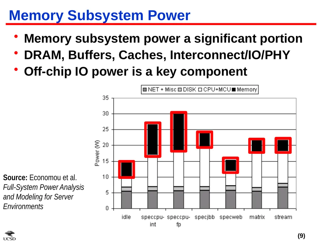
Memory Subsystem Power Memory subsystem power a significant portion
DRAM, Buffers, Caches, Interconnect/IO/PHY
Off-chip IO power is a key component Source: Economou et al.
Full-System Power Analysis and Modeling for Server
Environments<br>
10
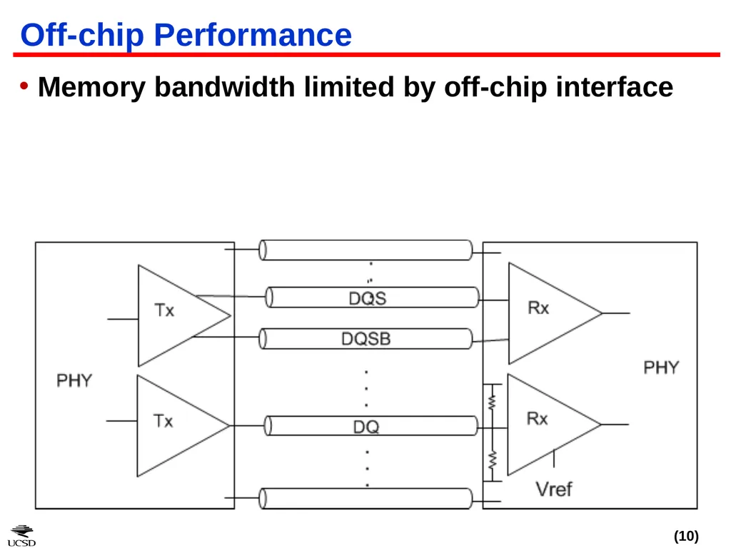
Off-chip Performance Memory bandwidth limited by off-chip interface<br>
11
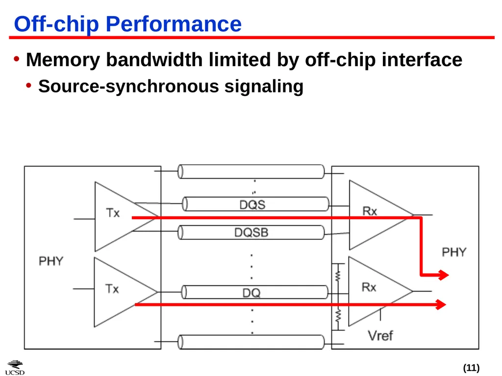
Off-chip Performance Memory bandwidth limited by off-chip interface
Source-synchronous signaling<br>
12
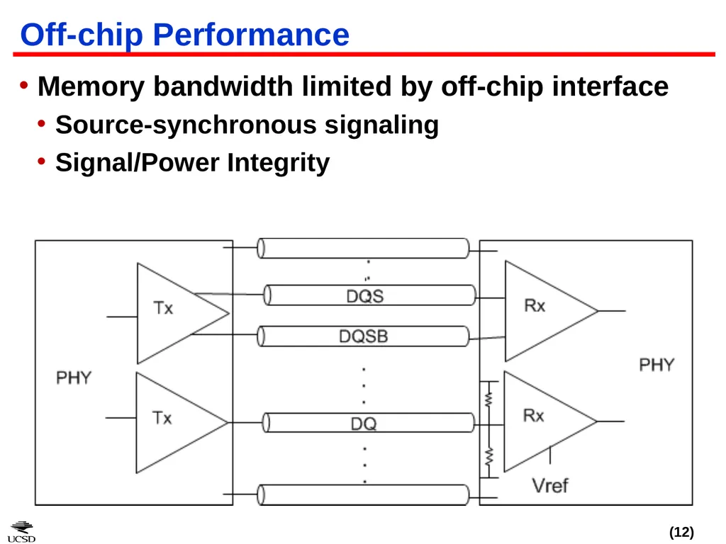
Off-chip Performance Memory bandwidth limited by off-chip interface
Source-synchronous signaling
Signal/Power Integrity<br>
13
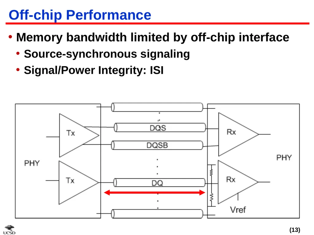
Off-chip Performance Memory bandwidth limited by off-chip interface
Source-synchronous signaling
Signal/Power Integrity: ISI<br>
14
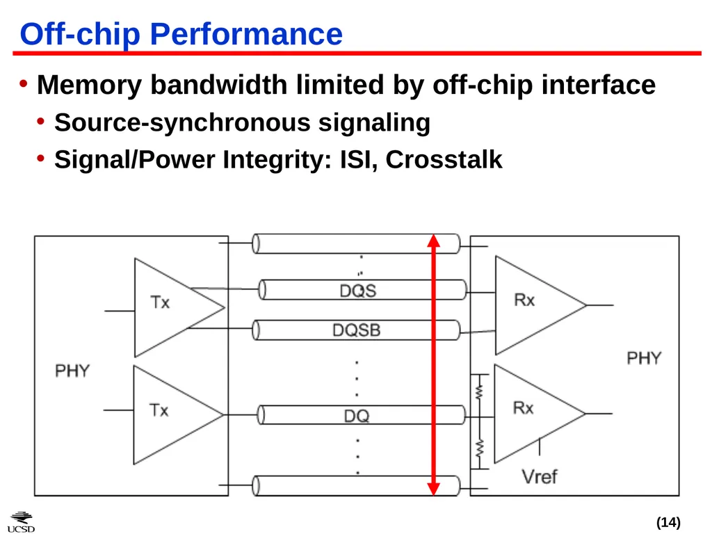
Off-chip Performance Memory bandwidth limited by off-chip interface
Source-synchronous signaling
Signal/Power Integrity: ISI, Crosstalk<br>
15
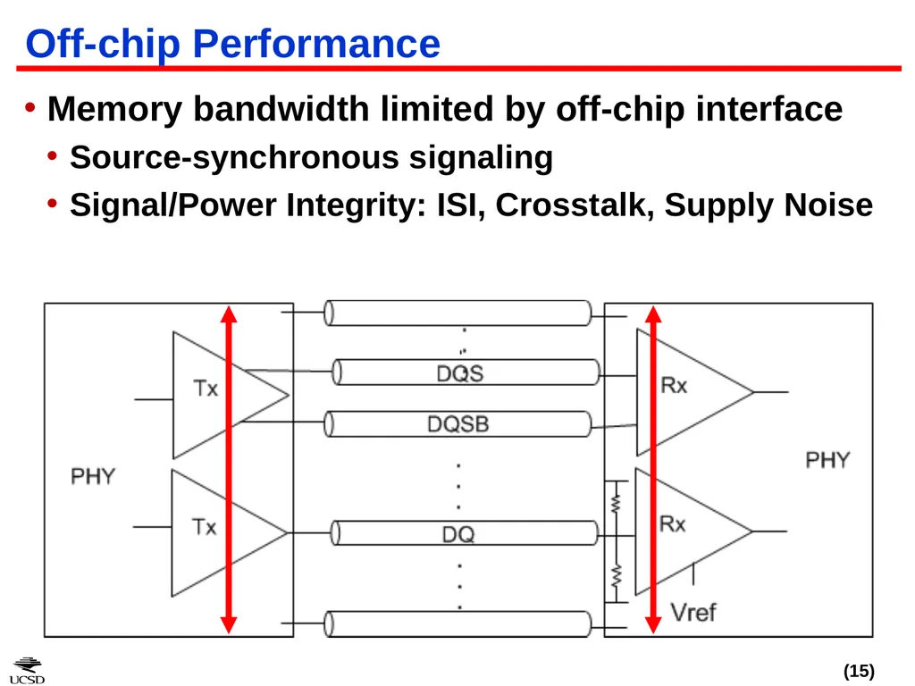
Off-chip Performance Memory bandwidth limited by off-chip interface
Source-synchronous signaling
Signal/Power Integrity: ISI, Crosstalk, Supply Noise<br>
16
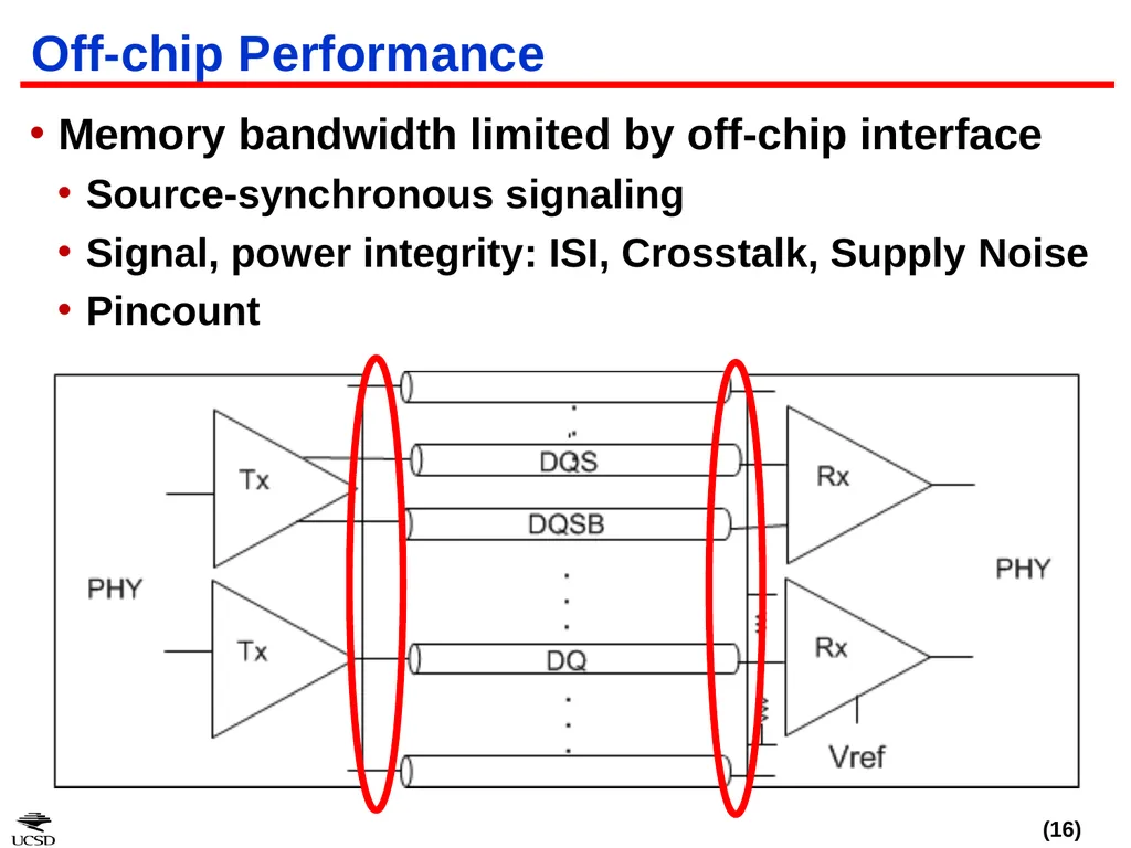
Off-chip Performance Memory bandwidth limited by off-chip interface
Source-synchronous signaling
Signal, power integrity: ISI, Crosstalk, Supply Noise
Pincount<br>
17
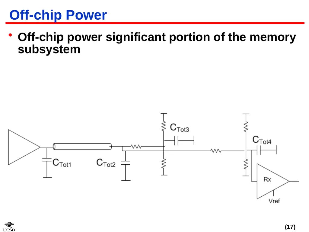
Off-chip Power Off-chip power significant portion of the memory subsystem<br>
18
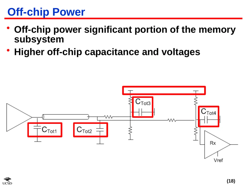
Off-chip Power Off-chip power significant portion of the memory subsystem
Higher off-chip capacitance and voltages<br>
19
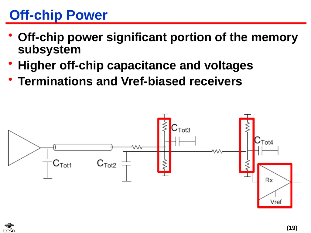
Off-chip Power Off-chip power significant portion of the memory subsystem
Higher off-chip capacitance and voltages
Terminations and Vref-biased receivers<br>
20
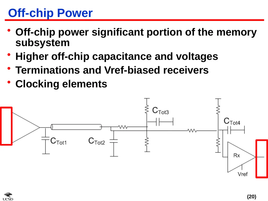
Off-chip Power Off-chip power significant portion of the memory subsystem
Higher off-chip capacitance and voltages
Terminations and Vref-biased receivers
Clocking elements<br>
21
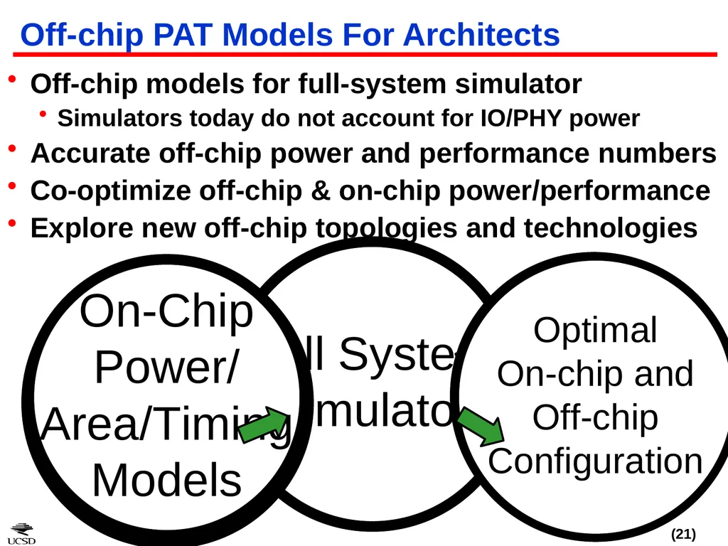
Off-chip PAT Models For Architects Off-chip models for full-system simulator
Simulators today do not account for IO/PHY power
Accurate off-chip power and performance numbers
Co-optimize off-chip & on-chip power/performance
Explore new off-chip topologies and technologies<br>
22
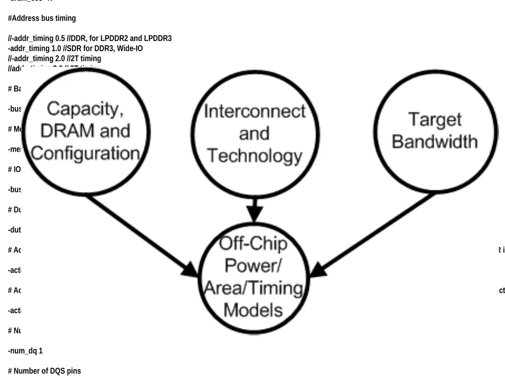
CACTI-IO CACTI well known for memory architects
CACTI-IO includes off-chip PAT models
CACTI-IO config file includes off-chip parameters
CACTI-IO Tech Report available # Memory State (R=Read, W=Write, I=Idle or S=Sleep)
//-iostate "R"
-iostate "W"
//-iostate "I"
//-iostate "S"
# Is ECC Enabled (Y=Yes, N=No)
-dram_ecc "N"
#Address bus timing
//-addr_timing 0.5 //DDR, for LPDDR2 and LPDDR3
-addr_timing 1.0 //SDR for DDR3, Wide-IO
//-addr_timing 2.0 //2T timing
//addr_timing 3.0 // 3T timing
# Bandwidth (Gbytes per second, this is the effective bandwidth)
-bus_bw 12.8 GBps
# Memory Density (Gbit per memory/DRAM die)
-mem_density 2 Gb
# IO frequency (MHz) (frequency of the external memory interface).
-bus_freq 800 MHz
# Duty Cycle (fraction of time in the Memory State defined above)
-duty_cycle 1.0
# Activity factor for Data (0->1 transitions) per cycle (for DDR, need to account for the higher activity in this parameter. E.g. max. activity factor for DDR is 1.0, for SDR is 0.5)
-activity_dq 1.0
# Activity factor for Control/Address (0->1 transitions) per cycle (for DDR, need to account for the higher activity in this parameter. E.g. max. activity factor for DDR is 1.0, for SDR is 0.5)
-activity_ca 0
# Number of DQ pins
-num_dq 1
# Number of DQS pins
-num_dqs 0 //8 differential pairs
# Number of CA pins
-num_ca 0
# Number of CLK pins
-num_clk 2 //1 differential pair
# Number of Physical Ranks
-num_mem_dq 2 //Number of ranks (loads on DQ and DQS) per DIMM or buffer chip
# Width of the Memory Data Bus
-mem_data_width 1 //x4 or x8 or x16 or x32 memories<br>
23
Agenda Introduction
Need for off-chip power-area-timing models
CACTI-IO Models
Case Studies using CACTI-IO:
High-capacity DDR3 configurations
3-D Stacking
BOOM: LPDDRx for servers
Summary<br>
24
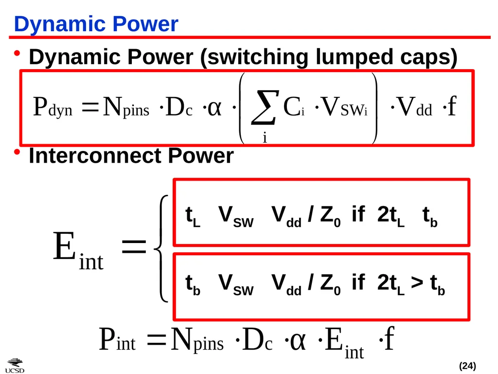
Dynamic Power Dynamic Power (switching lumped caps)
Interconnect Power tL VSW Vdd / Z0 if 2tL tb tb VSW Vdd / Z0 if 2tL > tb<br>
25
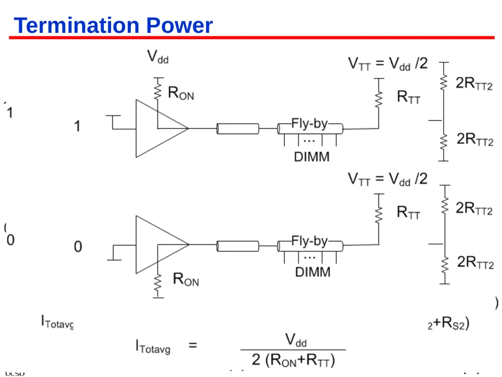
Termination Power DQ:
Multi rank
Few termination types
READ and WRITE
Assume 50% 0’s, 1’s
Includes Rx, Tx
CA:
Fly-by
VDD/2 termination<br>
26
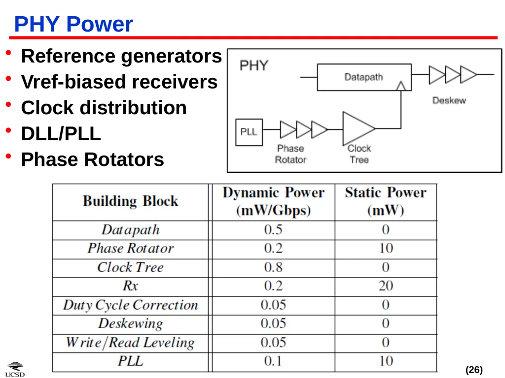
PHY Power Reference generators
Vref-biased receivers
Clock distribution
DLL/PLL
Phase Rotators<br>
27
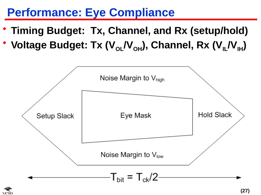
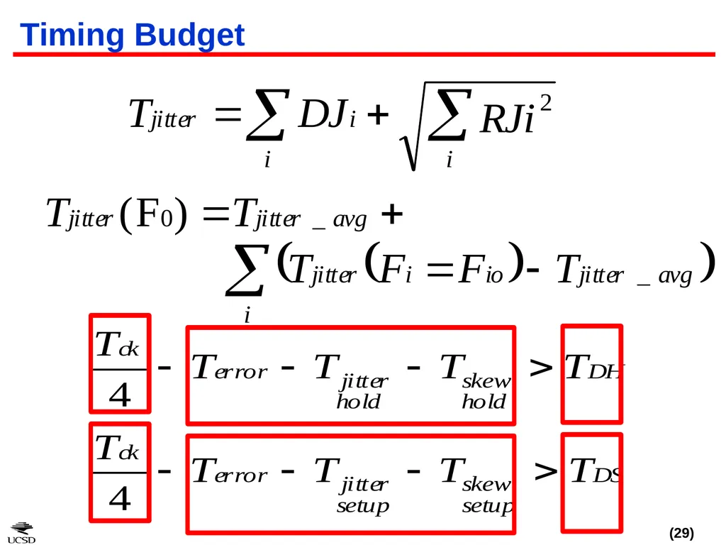
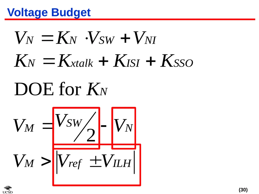
Performance: Eye Compliance Timing Budget: Tx, Channel, and Rx (setup/hold)
Voltage Budget: Tx (VOL/VOH), Channel, Rx (VIL/VIH)<br>
28
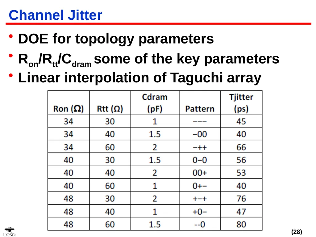
Channel Jitter DOE for topology parameters
Ron/Rtt/Cdram some of the key parameters
Linear interpolation of Taguchi array<br>
31
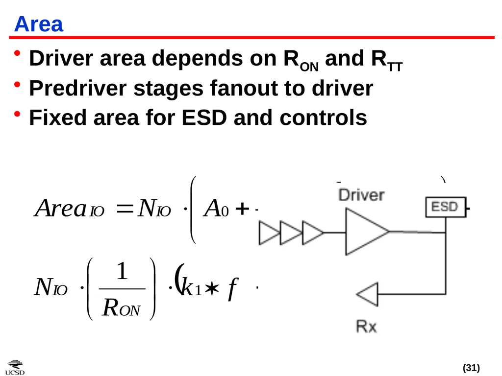
Area Driver area depends on RON and RTT
Predriver stages fanout to driver
Fixed area for ESD and controls<br>
32
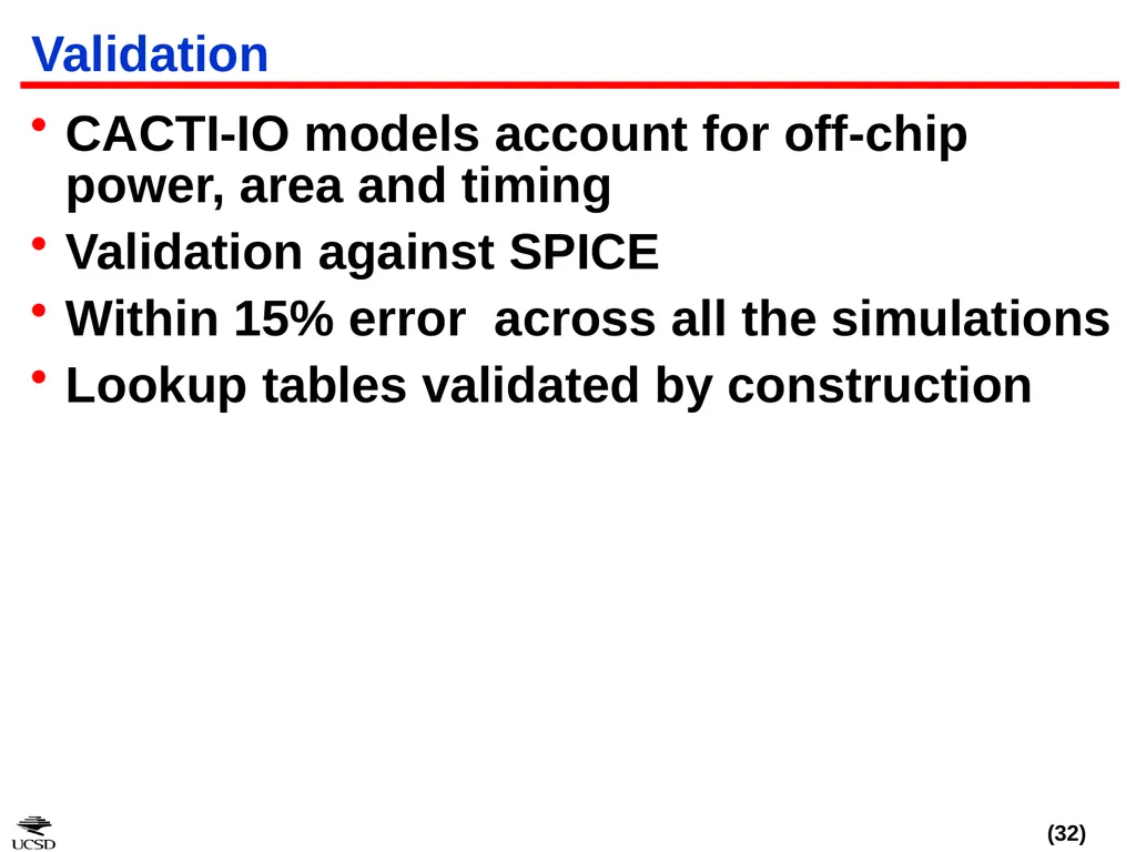
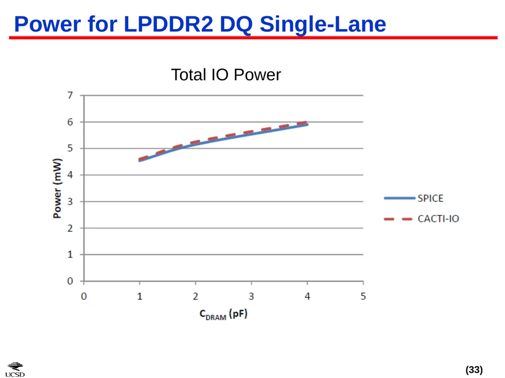
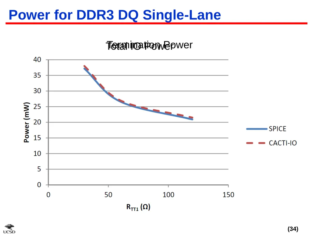
Validation CACTI-IO models account for off-chip power, area and timing
Validation against SPICE
Within 15% error across all the simulations
Lookup tables validated by construction<br>
33
Power for LPDDR2 DQ Single-Lane Total IO Power<br>
34
Power for DDR3 DQ Single-Lane Termination Power Total IO Power<br>
35
Agenda Introduction
Need for off-chip power-area-timing models
CACTI-IO Models
Case Studies using CACTI-IO:
High-capacity DDR3 configurations
3-D Stacking
BOOM: LPDDRx for servers
Summary<br>
36
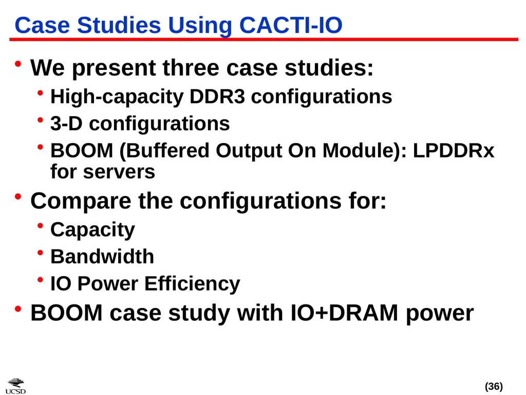
Case Studies Using CACTI-IO We present three case studies:
High-capacity DDR3 configurations
3-D configurations
BOOM (Buffered Output On Module): LPDDRx for servers
Compare the configurations for:
Capacity
Bandwidth
IO Power Efficiency
BOOM case study with IO+DRAM power<br>
37
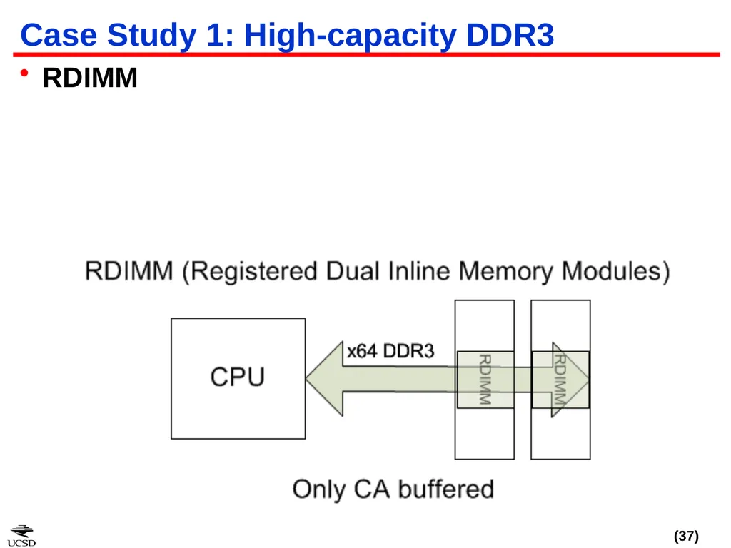
Case Study 1: High-capacity DDR3 RDIMM<br>
38
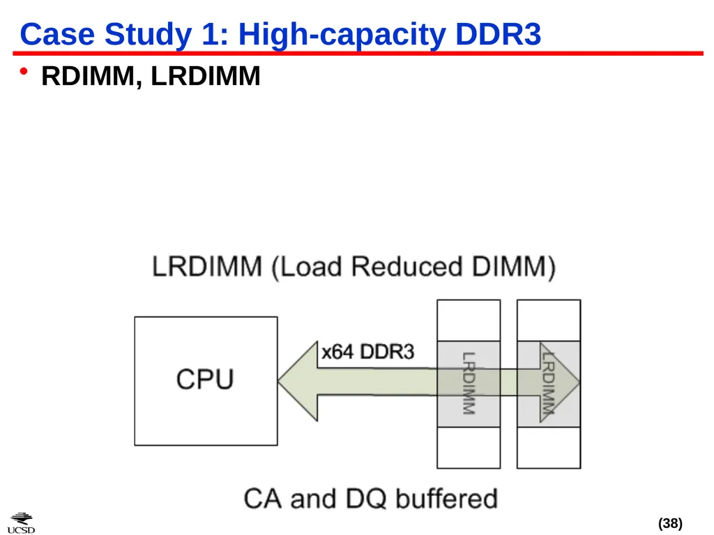
Case Study 1: High-capacity DDR3 RDIMM, LRDIMM<br>
39
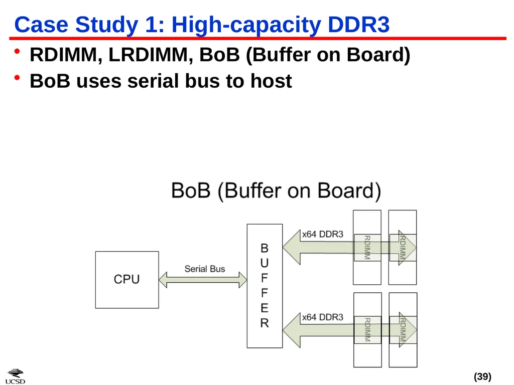
Case Study 1: High-capacity DDR3 RDIMM, LRDIMM, BoB (Buffer on Board)
BoB uses serial bus to host<br>
40
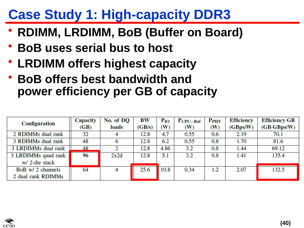
Case Study 1: High-capacity DDR3 RDIMM, LRDIMM, BoB (Buffer on Board)
BoB uses serial bus to host
LRDIMM offers highest capacity
BoB offers best bandwidth and power efficiency per GB of capacity<br>
41
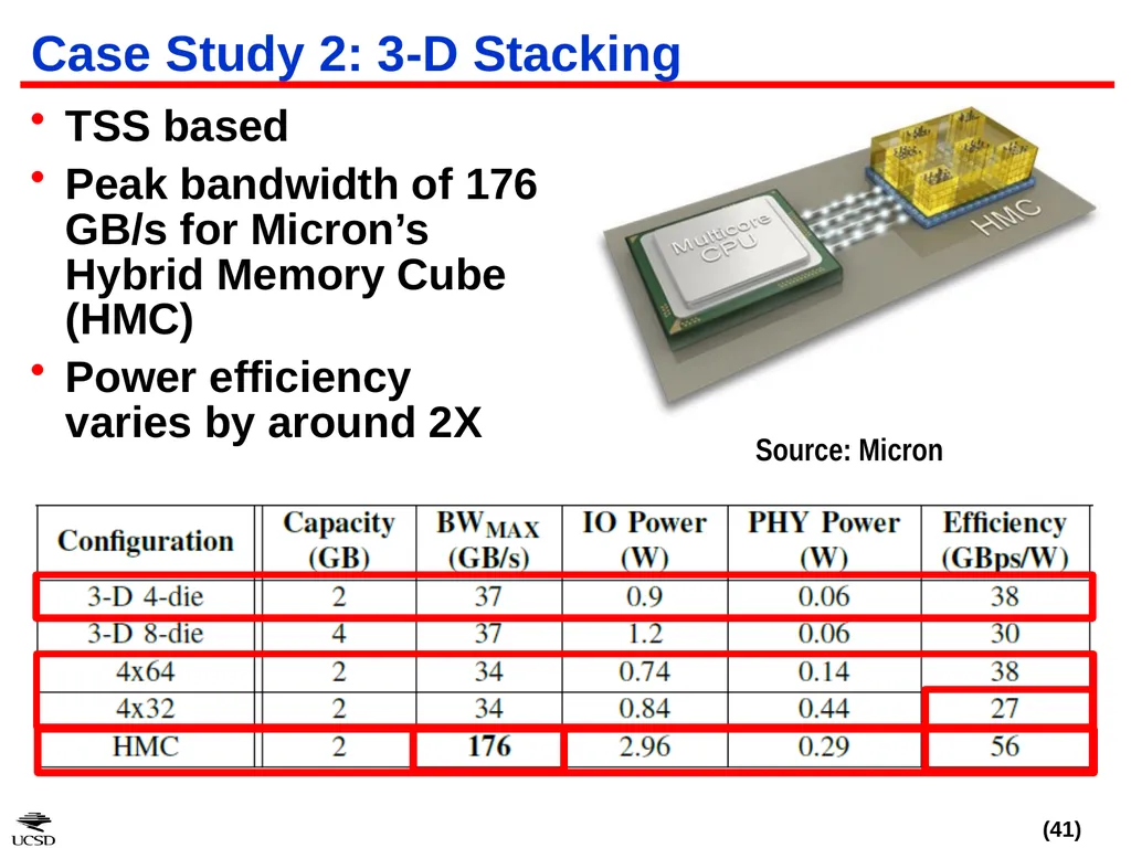
Case Study 2: 3-D Stacking TSS based
Peak bandwidth of 176 GB/s for Micron’s Hybrid Memory Cube (HMC)
Power efficiency varies by around 2X Source: Micron<br>
42
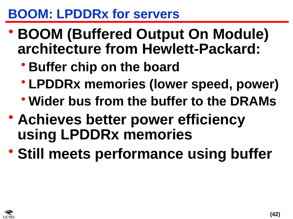
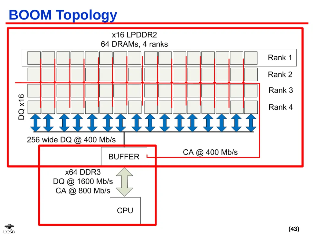
BOOM: LPDDRx for servers BOOM (Buffered Output On Module) architecture from Hewlett-Packard:
Buffer chip on the board
LPDDRx memories (lower speed, power)
Wider bus from the buffer to the DRAMs
Achieves better power efficiency using LPDDRx memories
Still meets performance using buffer<br>
44
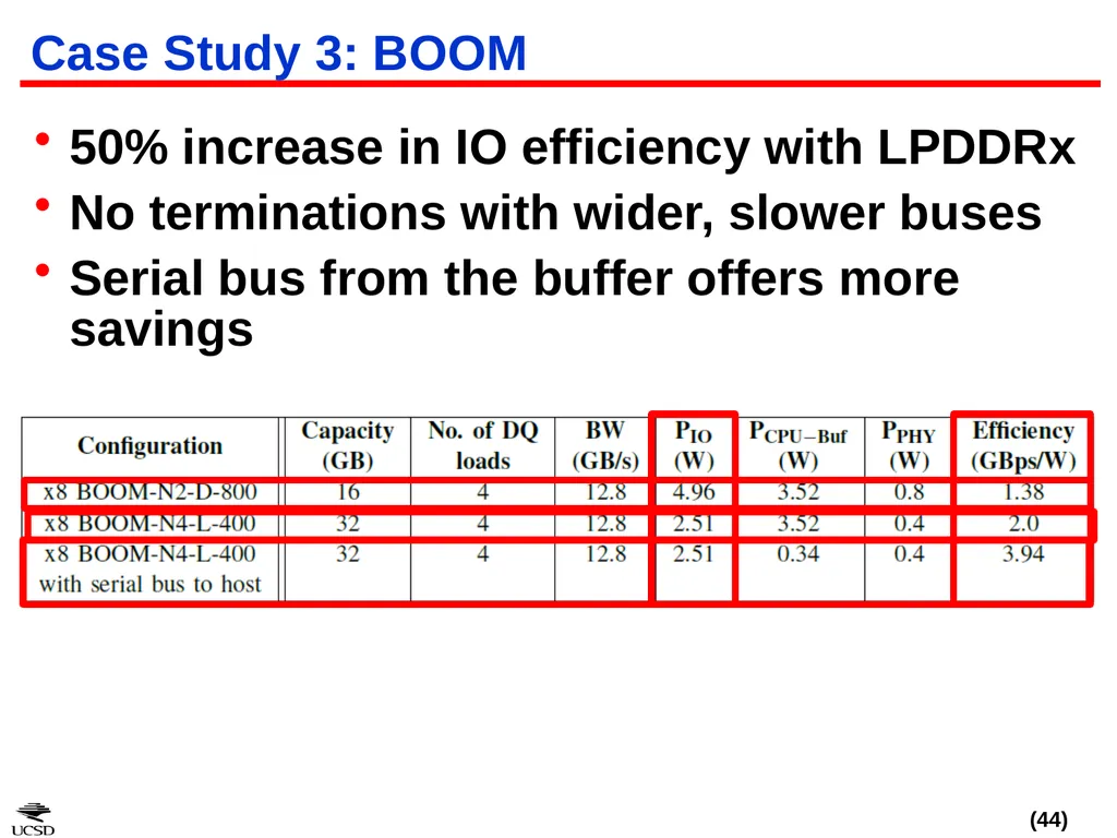
Case Study 3: BOOM 50% increase in IO efficiency with LPDDRx
No terminations with wider, slower buses
Serial bus from the buffer offers more savings<br>
45
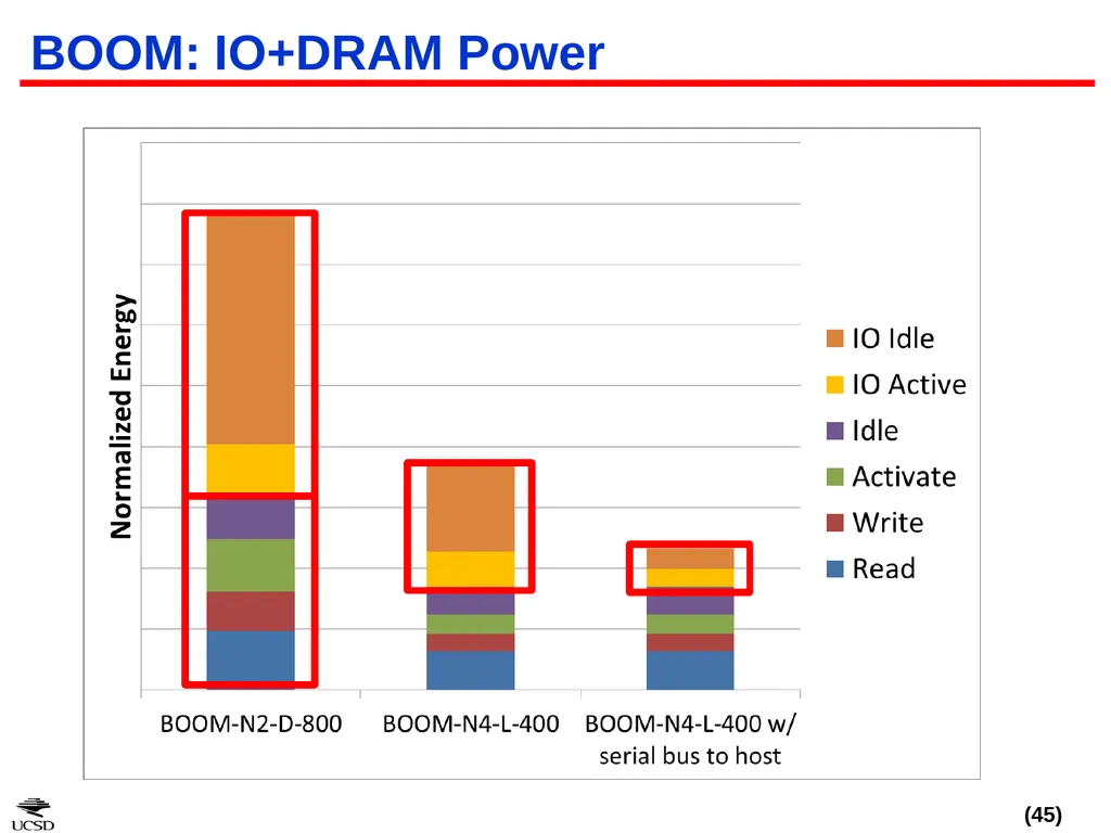
BOOM: IO+DRAM Power<br>
46
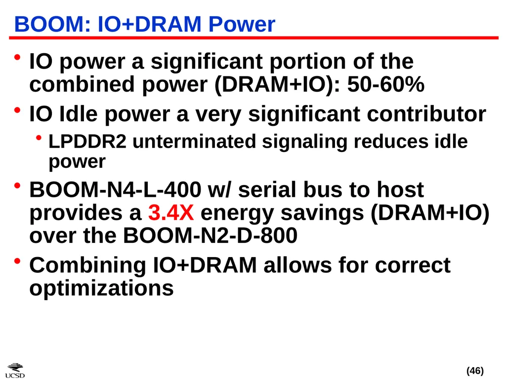
BOOM: IO+DRAM Power IO power a significant portion of the combined power (DRAM+IO): 50-60%
IO Idle power a very significant contributor
LPDDR2 unterminated signaling reduces idle power
BOOM-N4-L-400 w/ serial bus to host provides a 3.4X energy savings (DRAM+IO) over the BOOM-N2-D-800
Combining IO+DRAM allows for correct optimizations<br>
47
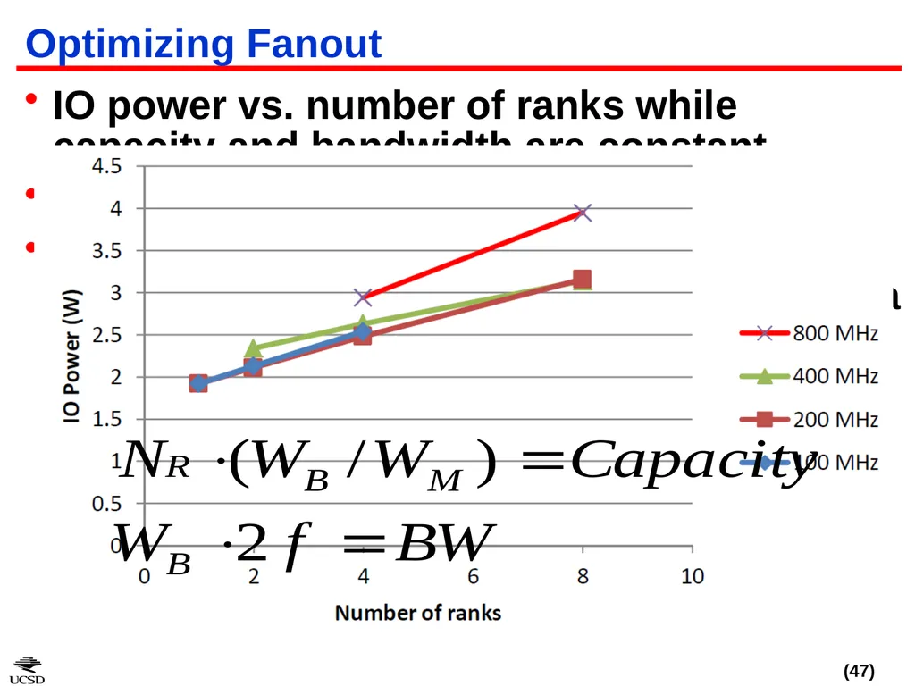
Optimizing Fanout IO power vs. number of ranks while capacity and bandwidth are constant
Slower and wider provides better power
Die area and clock distribution goes up as bus gets wider, so 200-400MHz seems like a sweet spot<br>
48
Agenda Introduction
Need for off-chip power-area-timing models
CACTI-IO Models
Case Studies using CACTI-IO:
High-capacity DDR3 configurations
3-D Stacking
BOOM: LPDDRx for servers
Summary<br>
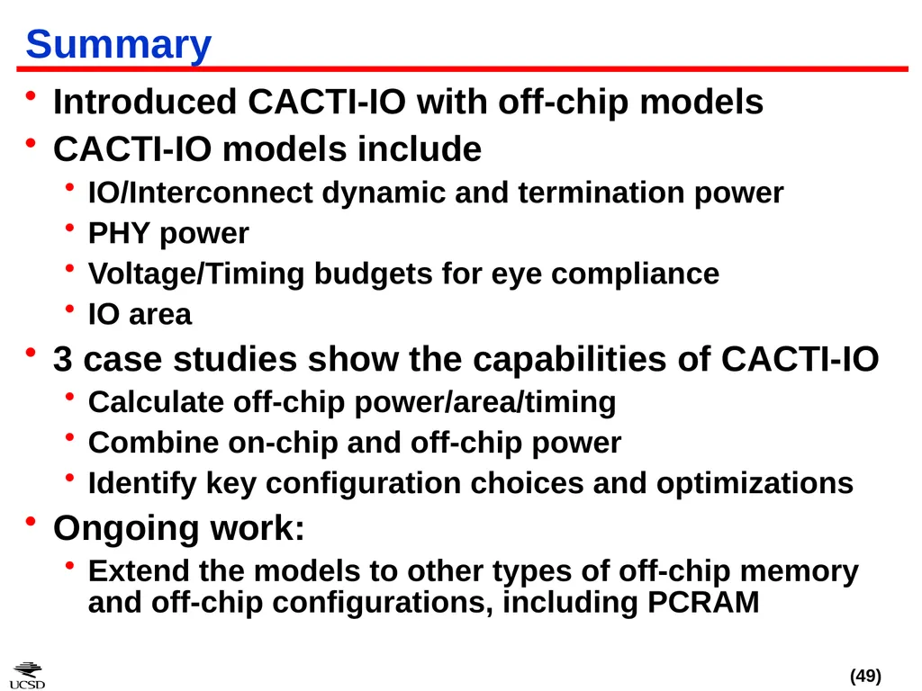
49
Summary Introduced CACTI-IO with off-chip models
CACTI-IO models include
IO/Interconnect dynamic and termination power
PHY power
Voltage/Timing budgets for eye compliance
IO area
3 case studies show the capabilities of CACTI-IO
Calculate off-chip power/area/timing
Combine on-chip and off-chip power
Identify key configuration choices and optimizations
Ongoing work:
Extend the models to other types of off-chip memory and off-chip configurations, including PCRAM<br>