Scanning Probe Microscopythe Scanning Tunneling Microscope Scanning Probe Microscopythe Scanning Tunneling Microscope The best optical microscopes can see structures in the 200 400 nm range, at their limits of resolution. The STM can
"Scanning Probe Microscopy—the Scanning Tunneling" is the property of its rightful owner. Permission is granted to
download and print the materials on this website for personal, non-commercial use only, and to display it
on your personal computer provided you do not modify the materials and that you retain all copyright
notices contained in the materials. By downloading content from our website, you accept the terms of this
agreement.
Scanning Probe Microscopy—the Scanning Tunneling Microscope
The best optical microscopes can see structures in the 200 – 400 nm range, at their limits of resolution.
The STM can “see” structures on the order of 0.1 nm [atoms!]—another SPM, the AFM—can distinguish things on the order of 100 nm [large molecules].<br>
03
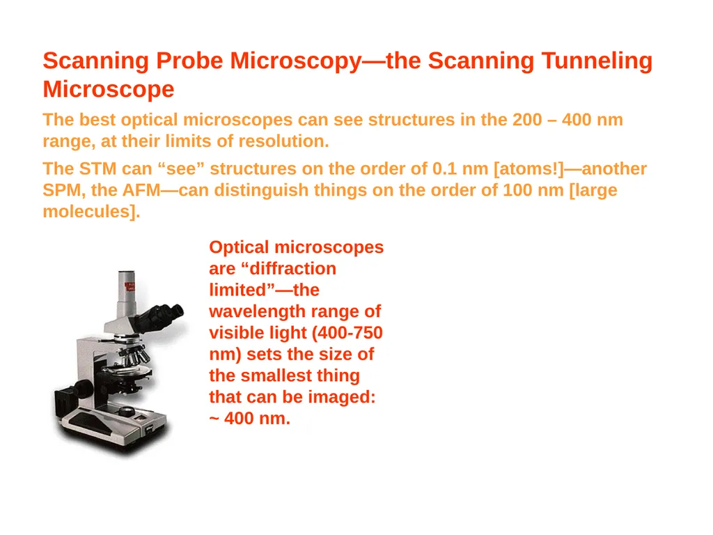
Optical microscopes are “diffraction limited”—the wavelength range of visible light (400-750 nm) sets the size of the smallest thing that can be imaged: ~ 400 nm. Scanning Probe Microscopy—the Scanning Tunneling Microscope
The best optical microscopes can see structures in the 200 – 400 nm range, at their limits of resolution.
The STM can “see” structures on the order of 0.1 nm [atoms!]—another SPM, the AFM—can distinguish things on the order of 100 nm [large molecules].<br>
04
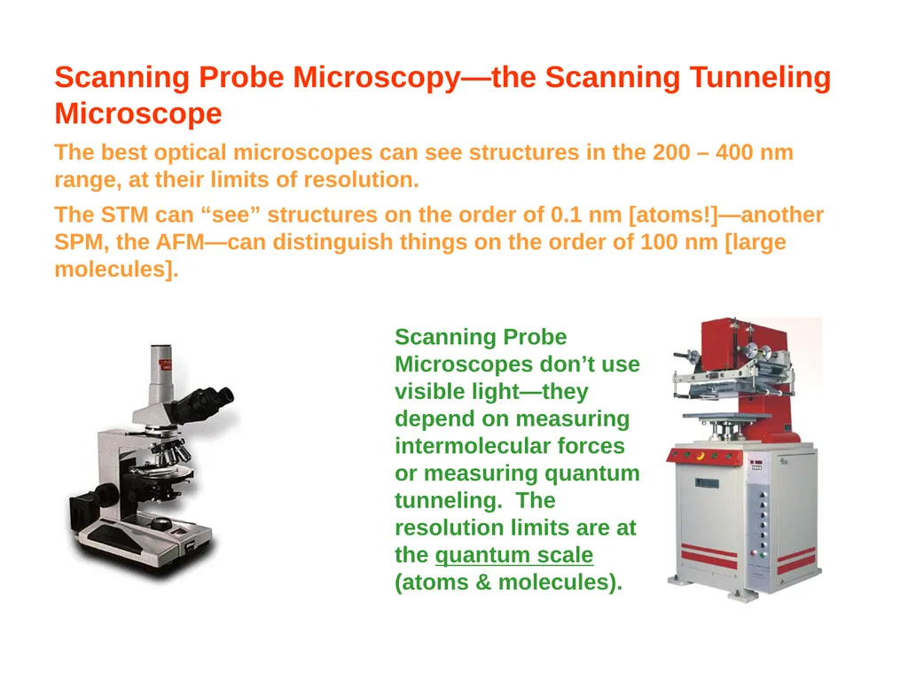
Scanning Probe Microscopes don’t use visible light—they depend on measuring intermolecular forces or measuring quantum tunneling. The resolution limits are at the quantum scale (atoms & molecules). Scanning Probe Microscopy—the Scanning Tunneling Microscope
The best optical microscopes can see structures in the 200 – 400 nm range, at their limits of resolution.
The STM can “see” structures on the order of 0.1 nm [atoms!]—another SPM, the AFM—can distinguish things on the order of 100 nm [large molecules].<br>
05
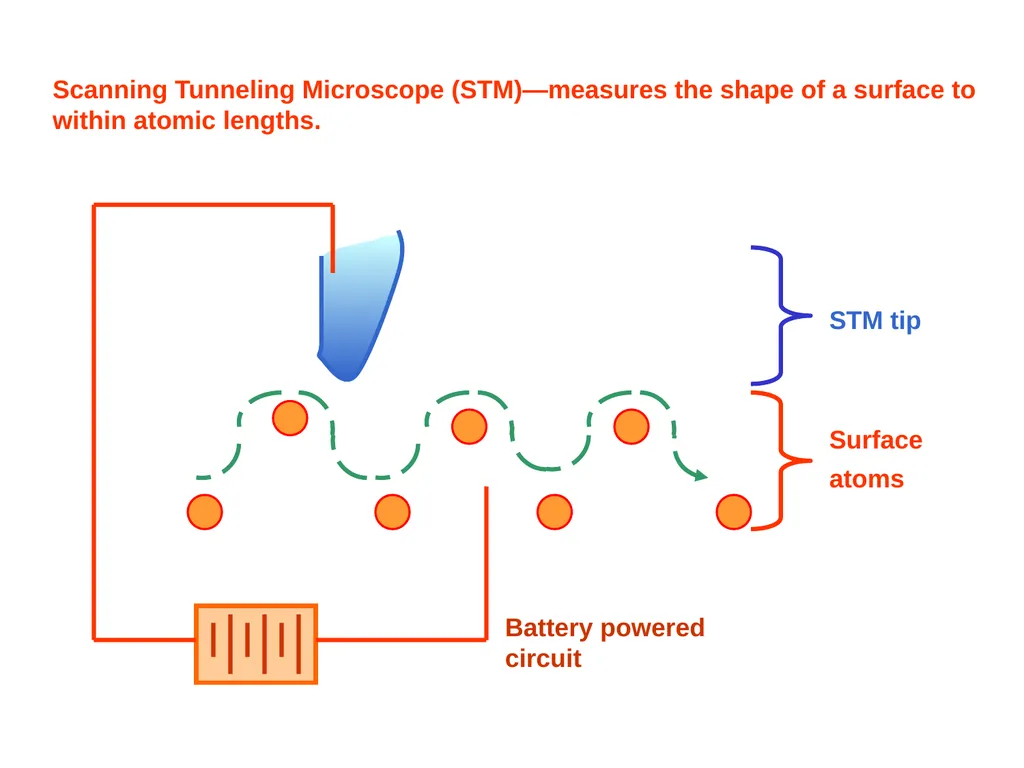
Scanning Tunneling Microscope (STM)—measures the shape of a surface to within atomic lengths.<br>
06
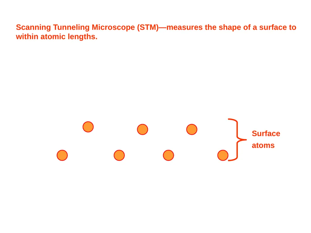
Scanning Tunneling Microscope (STM)—measures the shape of a surface to within atomic lengths. Surface
atoms<br>
07
Scanning Tunneling Microscope (STM)—measures the shape of a surface to within atomic lengths. Surface
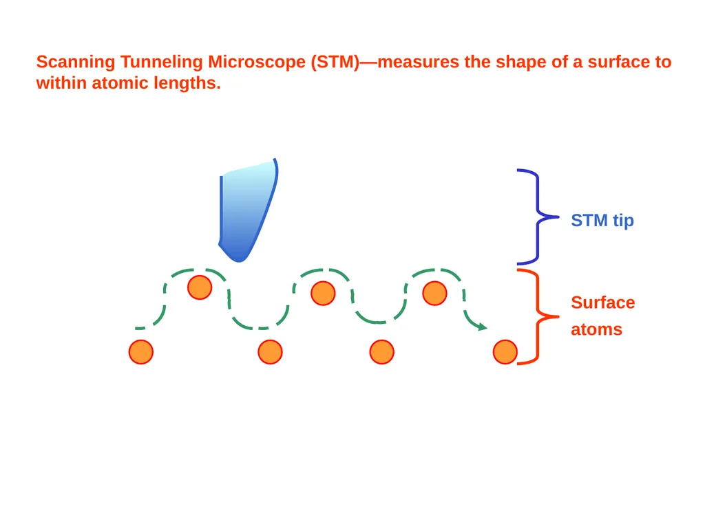
atoms STM tip<br>
08
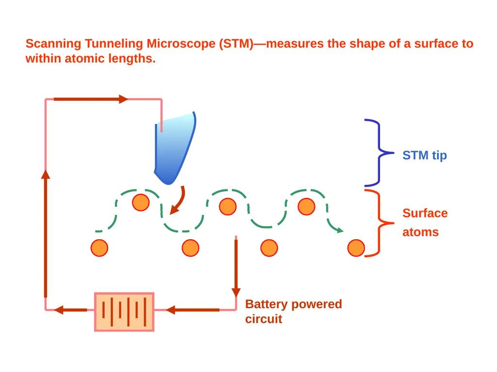
Scanning Tunneling Microscope (STM)—measures the shape of a surface to within atomic lengths. Surface
atoms STM tip Battery powered circuit<br>
09
Scanning Tunneling Microscope (STM)—measures the shape of a surface to within atomic lengths. Surface
atoms STM tip Battery powered circuit<br>
10
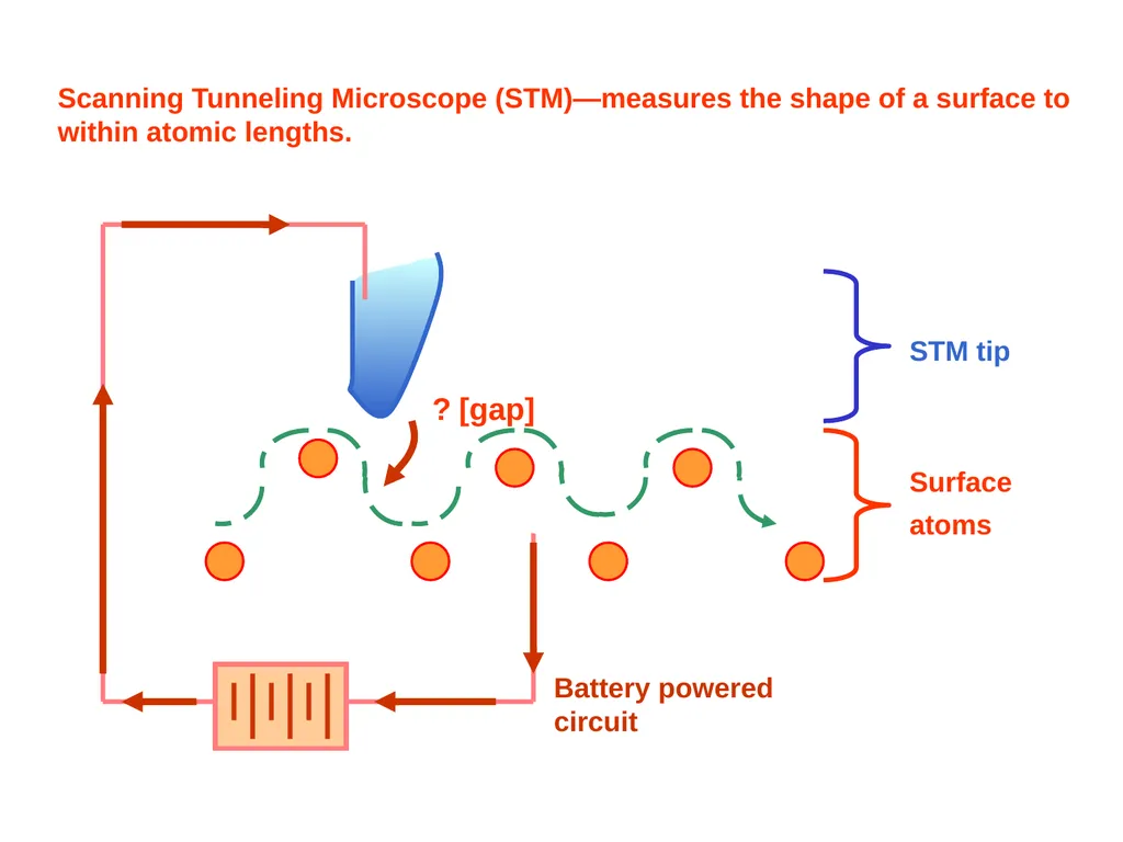
Scanning Tunneling Microscope (STM)—measures the shape of a surface to within atomic lengths. Surface
atoms STM tip Battery powered circuit ? [gap]<br>
11
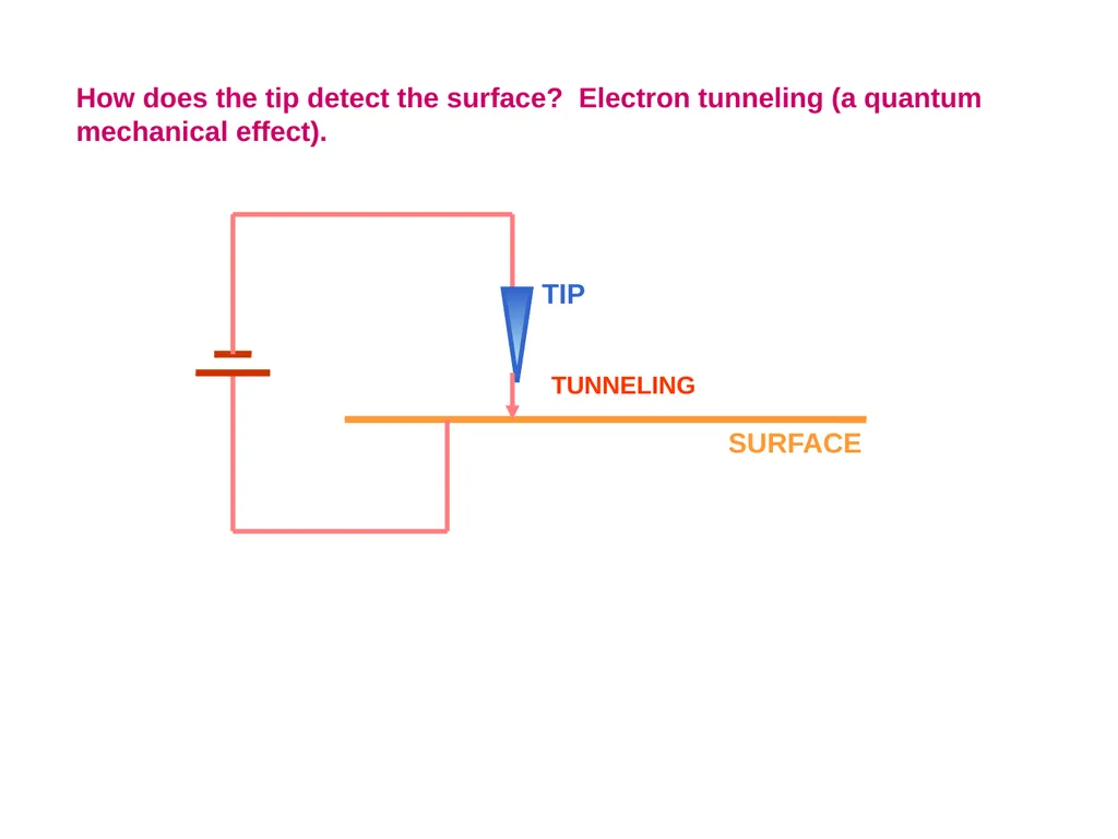
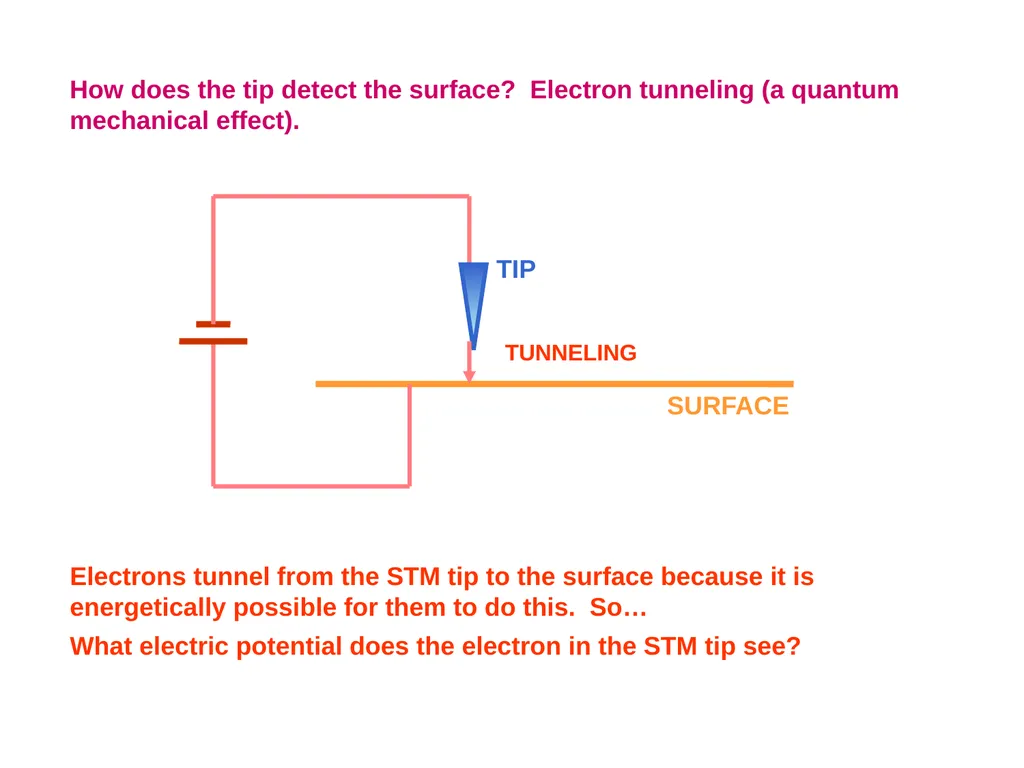
How does the tip detect the surface? Electron tunneling (a quantum mechanical effect). TUNNELING TIP SURFACE<br>
12
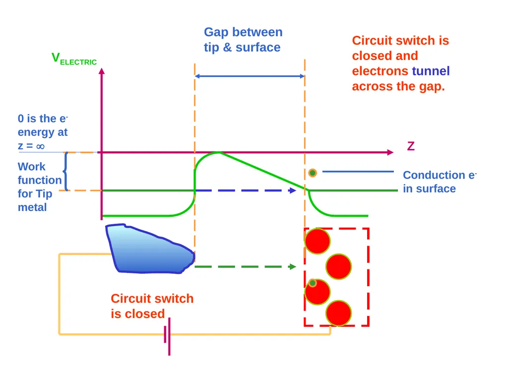
How does the tip detect the surface? Electron tunneling (a quantum mechanical effect). TUNNELING TIP SURFACE Electrons tunnel from the STM tip to the surface because it is energetically possible for them to do this. So…
What electric potential does the electron in the STM tip see?<br>
13
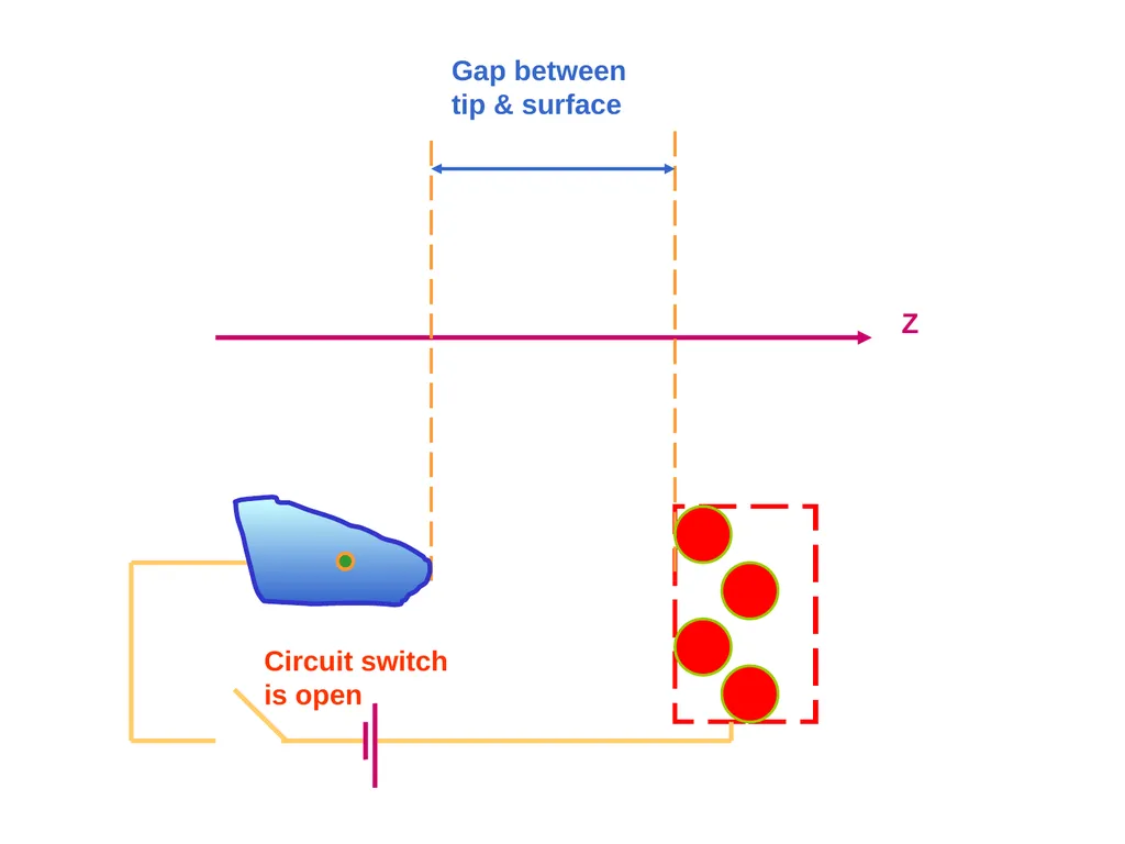
Z Gap between tip & surface Circuit switch is open<br>
14
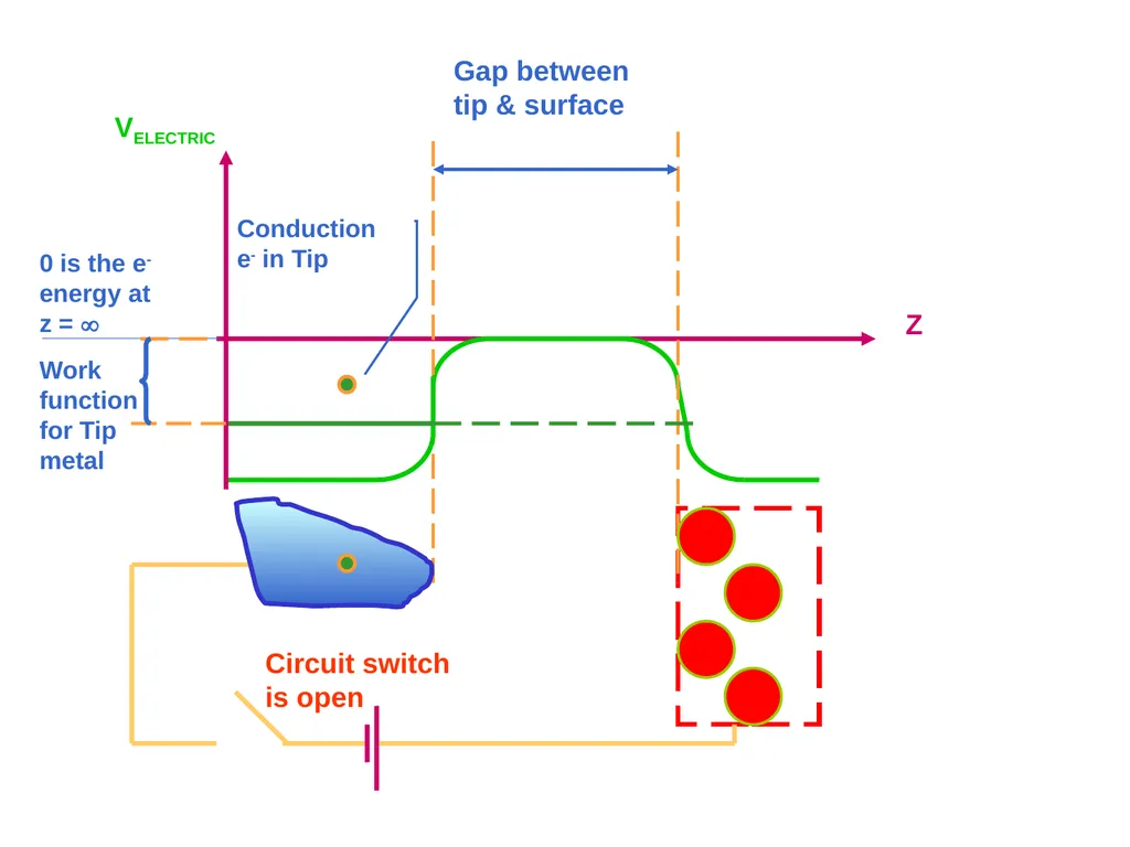
Z VELECTRIC 0 is the e- energy at z = Gap between tip & surface Circuit switch is open Work function for Tip metal Conduction e- in Tip<br>
15
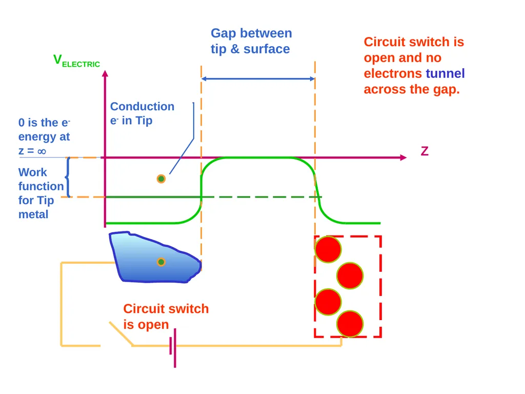
Z VELECTRIC 0 is the e- energy at z = Gap between tip & surface Circuit switch is open Work function for Tip metal Conduction e- in Tip Circuit switch is open and no electrons tunnel across the gap.<br>
16
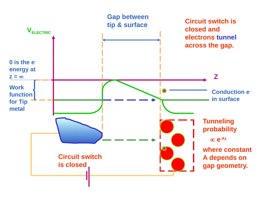
Z VELECTRIC 0 is the e- energy at z = Gap between tip & surface Circuit switch is closed Work function for Tip metal Circuit switch is closed and electrons tunnel across the gap. Conduction e- in surface<br>
17
Z VELECTRIC 0 is the e- energy at z = Gap between tip & surface Circuit switch is closed Work function for Tip metal Circuit switch is closed and electrons tunnel across the gap. Tunneling probability
e-Az
where constant A depends on gap geometry. Conduction e- in surface<br>
18
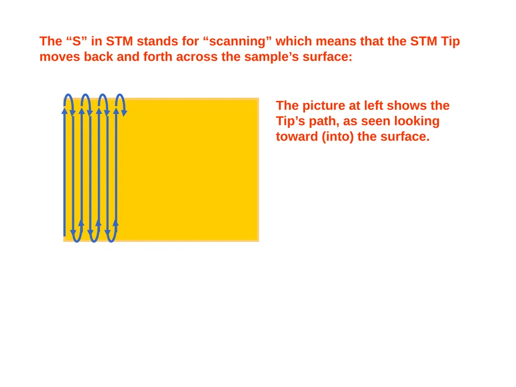
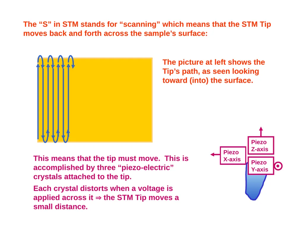
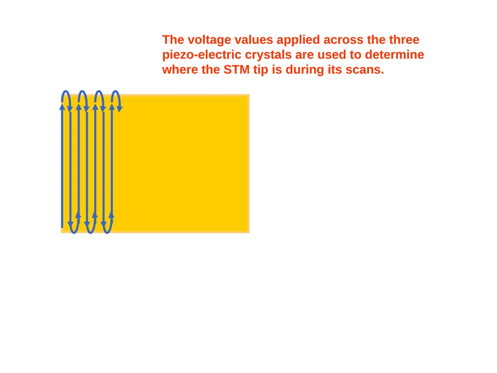
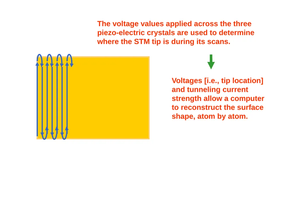
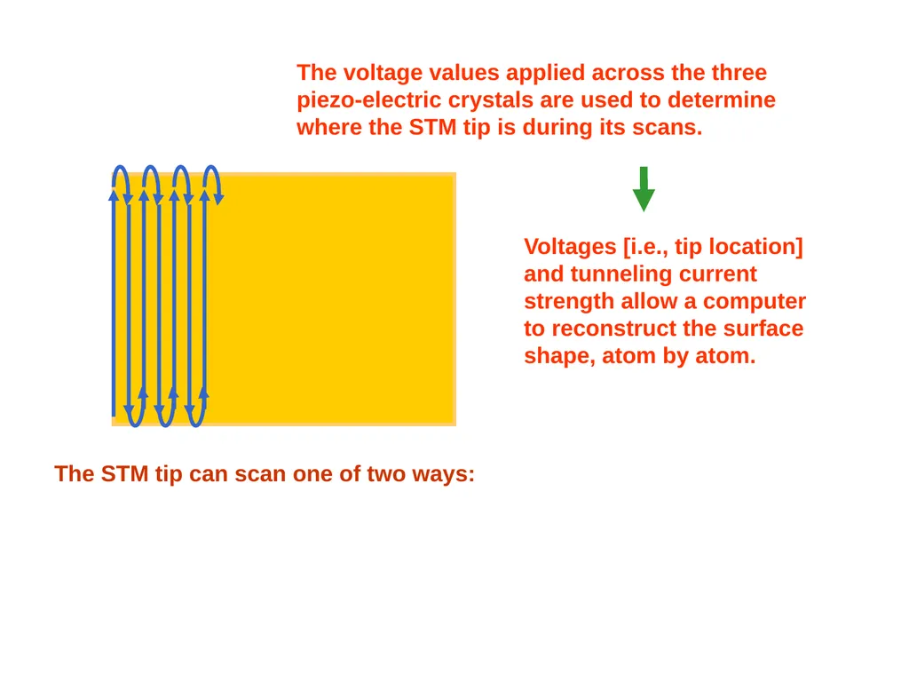
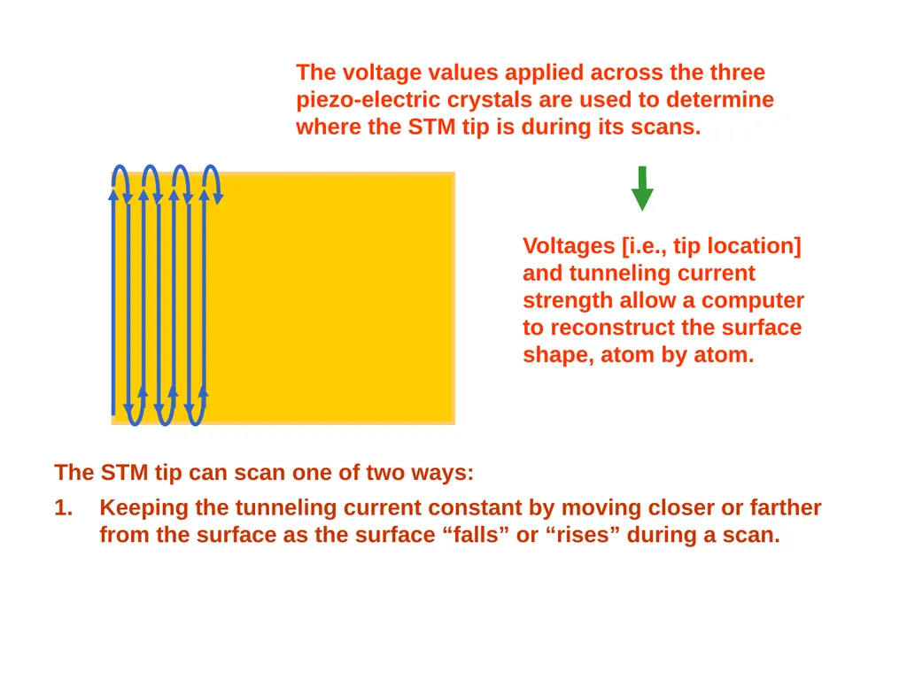
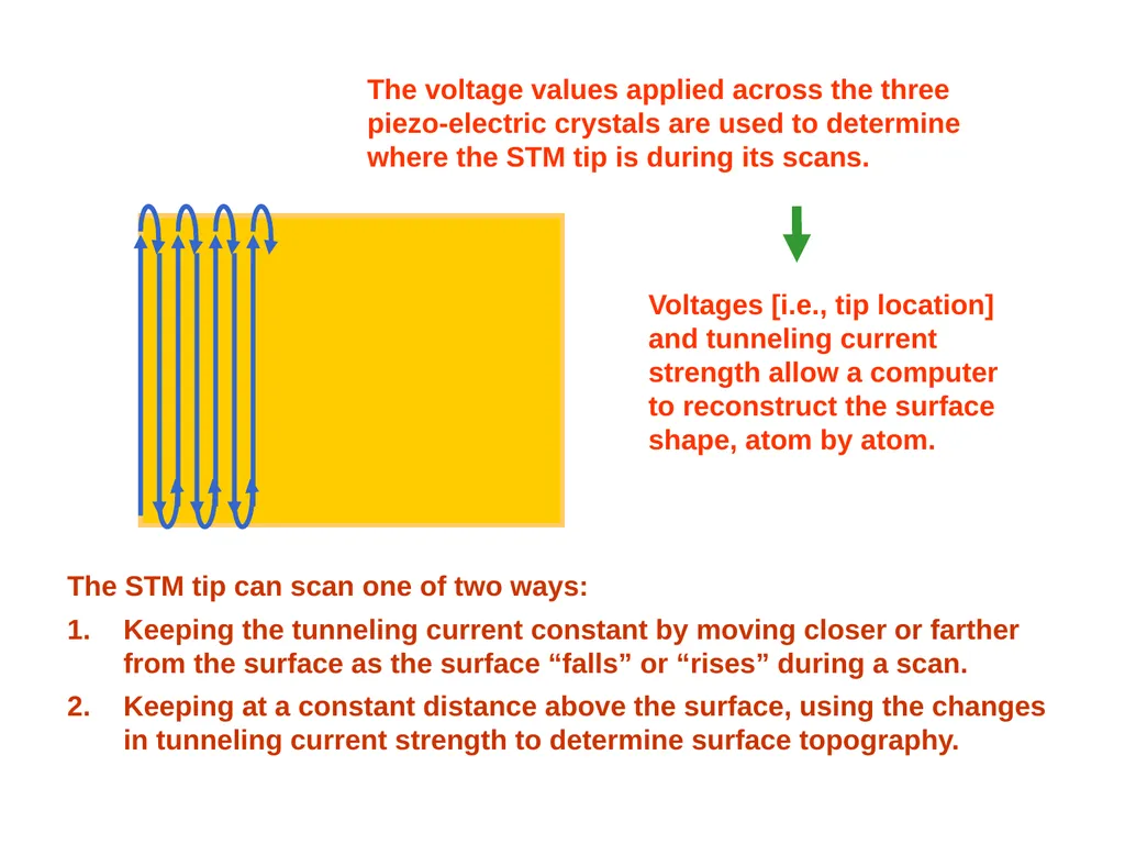
The “S” in STM stands for “scanning” which means that the STM Tip moves back and forth across the sample’s surface: The picture at left shows the Tip’s path, as seen looking toward (into) the surface.<br>
19
The “S” in STM stands for “scanning” which means that the STM Tip moves back and forth across the sample’s surface: The picture at left shows the Tip’s path, as seen looking toward (into) the surface. This means that the tip must move. This is accomplished by three “piezo-electric” crystals attached to the tip.
Each crystal distorts when a voltage is applied across it the STM Tip moves a small distance. Piezo Z-axis Piezo X-axis Piezo Y-axis <br>
20
The voltage values applied across the three piezo-electric crystals are used to determine where the STM tip is during its scans.<br>
21
The voltage values applied across the three piezo-electric crystals are used to determine where the STM tip is during its scans. Voltages [i.e., tip location] and tunneling current strength allow a computer to reconstruct the surface shape, atom by atom.<br>
22
The voltage values applied across the three piezo-electric crystals are used to determine where the STM tip is during its scans. Voltages [i.e., tip location] and tunneling current strength allow a computer to reconstruct the surface shape, atom by atom. The STM tip can scan one of two ways:<br>
23
The voltage values applied across the three piezo-electric crystals are used to determine where the STM tip is during its scans. Voltages [i.e., tip location] and tunneling current strength allow a computer to reconstruct the surface shape, atom by atom. The STM tip can scan one of two ways:
Keeping the tunneling current constant by moving closer or farther from the surface as the surface “falls” or “rises” during a scan.<br>
24
The voltage values applied across the three piezo-electric crystals are used to determine where the STM tip is during its scans. Voltages [i.e., tip location] and tunneling current strength allow a computer to reconstruct the surface shape, atom by atom. The STM tip can scan one of two ways:
Keeping the tunneling current constant by moving closer or farther from the surface as the surface “falls” or “rises” during a scan.
Keeping at a constant distance above the surface, using the changes in tunneling current strength to determine surface topography.<br>
25
Using the STM in lab— Place the STM tip near the sample surface, by hand;
Use the z-axis piezo electric motor to bring the tip close to the surface (within an atomic radius)—so that tunneling begins;
Use the x-axis and y-axis piezo-electric motors to move the tip over a scan area.<br>
26
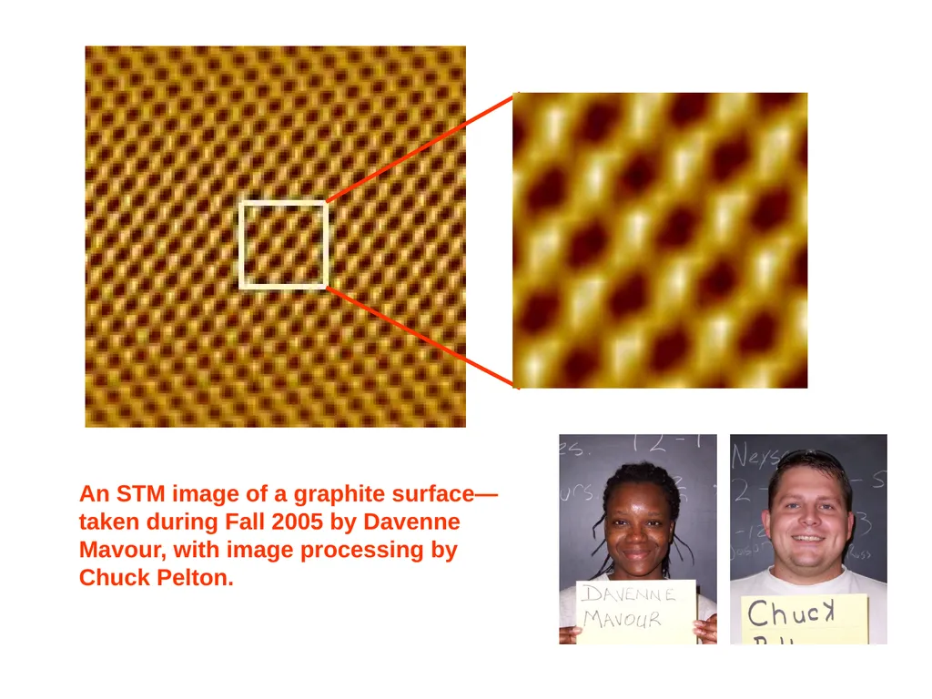
An STM image of a graphite surface—taken during Fall 2005 by Davenne Mavour, with image processing by Chuck Pelton.<br>