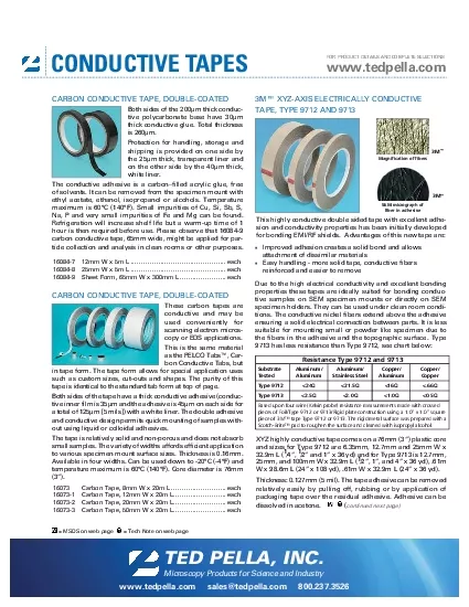
/
Transfer Printing of Conductive Thin-Films on PDMS with Soluble Substrates for Flexible Transfer Printing of Conductive Thin-Films on PDMS with Soluble Substrates for Flexible

Transfer Printing of Conductive Thin-Films on PDMS with Soluble Substrates for Flexible - PowerPoint Presentation

PrettyInPink
PrettyInPink . @PrettyInPink
Follow
342 views
Uploaded On 2022-08-02

Transfer Printing of Conductive Thin-Films on PDMS with Soluble Substrates for Flexible - PPT Presentation

7th International Electronic Conference on Sensors and Applications Steffen Hadeler Sebastian Bengsch Maren S Prediger Marc Christopher Wurz Institute of Micro Production Technology ID: 932299

manufacturing artmanufacturing ecog electrode artmanufacturing manufacturing electrode ecog introductionstate processmethodsconclusionoutlook art process characterization production thin dimensional test design hannover

Share:

Link:

Embed:

Download Presentation from below link

Download Presentation The PPT/PDF document "Transfer Printing of Conductive Thin-Fil..." is the property of its rightful owner. Permission is granted to download and print the materials on this web site for personal, non-commercial use only, and to display it on your personal computer provided you do not modify the materials and that you retain all copyright notices contained in the materials. By downloading content from our website, you accept the terms of this agreement.


Presentation Transcript

Slide1

Transfer Printing of Conductive Thin-Films on PDMS with Soluble Substrates for Flexible Biosensors

7th

International Electronic Conference on Sensors and

Applications

Steffen Hadeler,

Sebastian Bengsch, Maren S. Prediger, Marc Christopher Wurz

Slide2

Institute

of Micro Production TechnologyPZH - Hannover Centre for Production TechnologyLeibniz University Hannover, Lower Saxony, Germany

Introduction

IntroductionState of the artManufacturing ProcessMethodsConclusionOutlook

Slide3

Various sensors in medical technology have conductive

structuresIn this thesis: Focus on electrocorticography (ECOG)Invasive, Highly sensitiveMeasurement of

brain functions

Applications of ECoG:treatment of diseases like epilepsyBrain-Computer-InterfaceState of the art I IntroductionState of

the artManufacturing Process

MethodsConclusionOutlook

Slide4

Commercial

ECoG Electrodesplatinum wire and plates in PDMSAdvantage: the

long-term clinical experience

Disadvantage: rigidity, limited resolutionPublished ECoG Electrodesphotolithography and physical vapour deposition (PVD)on polyimide

Advantage: high resolutionDisadvantage: complex production in clean

roomState of the art II

IntroductionState of the artManufacturing ProcessMethodsConclusionOutlook

[2]

[1]

Slide5

C

ombine the advantages of the above methods Clinical long-term experience PDMSincrease resolution

reduction of electrode spacing

Manufacturing ProcessIntroductionState of the artManufacturing ProcessMethods

ConclusionOutlook

Slide6

Evaluation

of the developed manufacturing processMaterial characterizationAdhesion FlexibilityElectrical characterization

ConductivityImpedance Measurement

Demonstrator systemMethodsIntroductionState of the artManufacturing Process

MethodsConclusionOutlook

Slide7

Adhesion

cross cut test according to DIN EN ISO 2409platinum and gold

Platium poor adhesion

Gold better adhesionFlexibilityTensile test according to to DIN 53504 Different layer heights

Silicatization with NanoFlame

Material characterization

IntroductionState of the artManufacturing ProcessMethodsConclusionOutlook

Slide8

Conductivity

Four-point measurementBefore Transfer (

red)

After Transfer (grey)Different layer heightsElectrical characterization IIntroduction

State of the art

Manufacturing ProcessMethodsConclusion

Outlook

Slide9

Electrochemical

impedance measurementAs described in Nahvi et al. [3]

Sodium

chloride solution (9 mg/l)LCR meter HM9119 (Hameg Instruments GmbH)Electrode with 2 contacts, 1x1 mm

Electrical characterization II

IntroductionState of the

artManufacturing ProcessMethodsConclusionOutlook [3]

Slide10

Design

of an ECoG electrode array8 electrode contacts 1x1 mm²Supply lines 0,25 mm

isolated with PDMS

Design of a three-dimensional electrodeAdditive production of different casting mouldsDemonstrator systemIntroductionState of the art

Manufacturing ProcessMethodsConclusion

Outlook

Slide11

New

manufacturing process developedHigh resolution through thin film technologyUse of PDMS

Various studies for

optimizationAdhesionFlexibilityConductanceDesign of a demonstratortwo-dimensional three-dimensionalConclusionIntroduction

State of the

artManufacturing ProcessMethods

ConclusionOutlook

Slide12

Improvement

of the PVD processhigher resolution maskingMore electrode contactsRoll-

to-roll processthree-dimensional manufacturing

Better additive manufacturingpatient individual electrodesAdaptation for other implants and biosensorsOutlookIntroductionState of the

artManufacturing Process

MethodsConclusionOutlook

Slide13

Thank you for your attention

hadeler@impt.uni-hannover.de

Slide14

[1]

PMT Corporation: Cortac Grids & Strips. http://www.pmtcorp.com/cortac.html. Version: 06.05.2019[2] Rubehn, Birthe ; Bosman, Conrado ; Oostenveld, Robert ; Fries, Pascal ; Stieglitz,

Thomas: A MEMS-based flexible multichannel ECoG-electrode array. In: Journal of neural

engineering 6 (2009), Nr. 3, S. 036003. [3] Nahvi, Mohammad S. ; Boroumand, Farhad A. ; Maghami, Mohammad H. ; Sodagar, Amir M. ; Shojaei, Amir ; Mirnajafi-Zadeh, Javad: Design, fabrication, and test of flexible thin-film microelectrode arrays for neural interfaces. 2017 IEEE 30th Canadian Conference on Electrical and Computer Engineering

Sources