/
Why the EU needs to invest in   chip design Why the EU needs to invest in   chip design

Why the EU needs to invest in chip design - PDF document

dandy
dandy . @dandy
Follow
342 views
Uploaded On 2021-10-08

Why the EU needs to invest in chip design - PPT Presentation

EUs central weakness regarding semiconductors This paper argues that the strong focus on establishing cuttingedge fabs in the EU is illadvised and the wrong rst step to meaningfully strengthen the E ID: 898459

https 2020 chip equipment 2020 https equipment chip semiconductor www fab semiconductors manufacturing fabs billion design europe 5nm nodes

Share:

Link:

Embed:

Download Presentation from below link

Download Pdf The PPT/PDF document "Why the EU needs to invest in chip des..." is the property of its rightful owner. Permission is granted to download and print the materials on this web site for personal, non-commercial use only, and to display it on your personal computer provided you do not modify the materials and that you retain all copyright notices contained in the materials. By downloading content from our website, you accept the terms of this agreement.


Presentation Transcript

1 Why the EU needs to invest in chip des
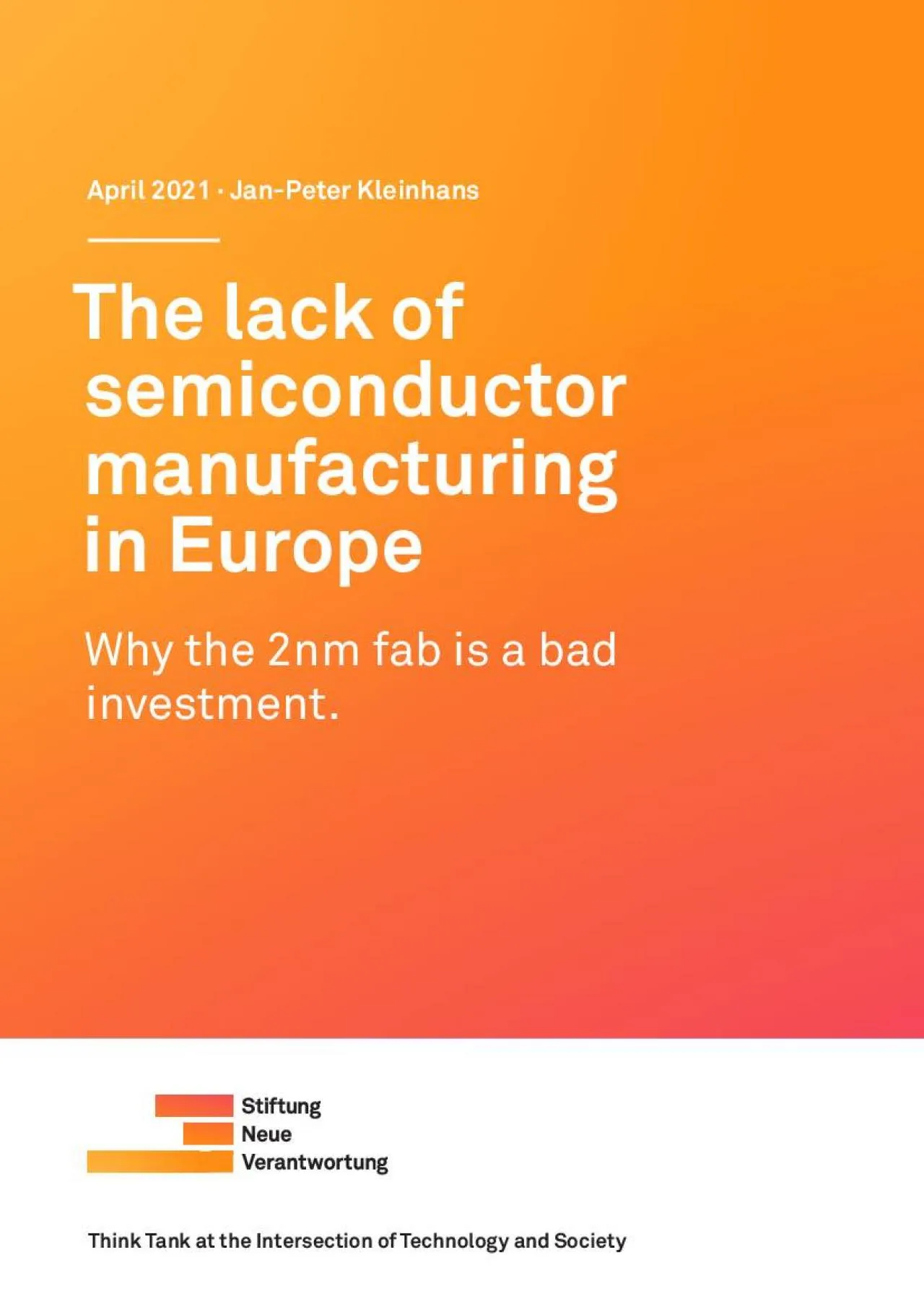
Why the EU needs to invest in chip design EUÕs central weakness regarding semiconductors. This paper argues that the strong focus on establishing cutting-edge fabs in the EU is ill-advised and the wrong !rst ste

2 p to meaningfully strengthen the EUÕs se
p to meaningfully strengthen the EUÕs semicon Skyrocketing costs of new fabs: Capital expenditure for a modern (5nm) fab is close to US$20 billion with annual operating expenditures of more than US$1 billion.20 The

3 skyrocketing costs mainly stem from inc
skyrocketing costs mainly stem from increasingly complex and ex-pensive manufacturing equipment.21 Part of the rising operating expenditures are electricity costs. For example, analysts estimated that TSMC account

4 ed for close to 5% of TaiwanÕs electrici
ed for close to 5% of TaiwanÕs electricity consumption in 2019.22¥ High volume, high utilization: To amortize such a huge investment within a few years, a fab needs high utilization rates. UMC, the second largest f

5 oundry in Tai 36 (28nm FD-SOI37), and Gl
oundry in Tai 36 (28nm FD-SOI37), and Globalfoundries in Dresden, Germany38 (22nm FD-SOI). Globalfound-¥ 130nm in Corbeil-Essonnes, France) and NXP (ƶ140nm in Nijmegen, the Neth-erlands)41 operate these process n

6 odes. Although some of these nodes could
odes. Although some of these nodes could be considered ÒantiqueÓ by todayÕs standards for mobile chips and processors, the nodes are in high demand for chips in automotive and industrial applications. !"ƶŽ180nmAl

7 most 50% of EuropeÕs total wafer capacit
most 50% of EuropeÕs total wafer capacity consists of nodes that are 180nm or larger. Although they were introduced more than 20 years ago, these nodes are still in use today for power semiconductors, sensors and o

8 ther types of analog semiconductors. In
ther types of analog semiconductors. In addition to the companies above, many specialty foundries such as X-FAB42 and United Monolithic Semiconductor (UMS), both with fabs in "ected in the spending on equipment ov

9 er the past 20 years (!gure 3). To keep
er the past 20 years (!gure 3). To keep pace with improving manufacturing processes, fabs must constantly expand capacity and invest in the next generation of manufacturing equipment. Thus, the amount of equipment

10 spending per region is a good proxy to a
spending per region is a good proxy to analyze which regions have seen the largest fab investments. In 2003, Europe was responsible for nearly 12% of all equipment spending, but in 2020, only 3% of equipment spendi

11 ng was in Europe. The global equipment m
ng was in Europe. The global equipment market grew from US$22 billion in 2003 to around US$69 bil-lion in 2020, but investment in manufacturing equipment in Europe was smaller in 2020 (US$2.4 billion) than in 2003

12 (US$2.56 billion).Figure 4 furthermore i
(US$2.56 billion).Figure 4 furthermore illustrates the long-term trend of cutting-edge wafer fabrica- tronics (SiC/GaN in Catania, Italy and GaN in Tours, France)46. As sensors, power and RF semiconductors are the

13 strong suite of the EUÕs major semicondu
strong suite of the EUÕs major semiconductor companies, Figure 4Figure 5 Ð Ð and information about Samsung building a cutting-edge fab in the US leaked this year.59 Samsung is asking for around US$1 billion in t

14 ax abatements and tax breaks.60 The US g
ax abatements and tax breaks.60 The US governmentÕs focus on wafer fabrication could be an economically viable strategy, because the US has the largest chip design industry in the world to create demand for these f

15 uture fabs. All the subsidies in the wor
uture fabs. All the subsidies in the world would not help to estab-lish a sustainable wafer fabrication ecosystem if there were no demand. The same is not the case for a potential EU foundry, however. Because of th

16 e lack of cutting-edge chip designs with
e lack of cutting-edge chip designs within Europe, the region would rely on foreign (US) chip design companies for orders. The question is, why would US fabless compa-nies choose to manufacture their chips not in S

17 outh Korea, Taiwan or the United States
outh Korea, Taiwan or the United States but in Europe? And why when the future cutting-edge EU fab is operated not by Samsung or TSMC but by an EU consortium61? A chip design is always based on a particular process

18 node from a certain companyÕs fab. One
node from a certain companyÕs fab. One cannot simply switch from TSMCÕs 5nm node to SamsungÕs 5nm node. If TSMC or Samsung operates cut-Figure 6 rity rationale for Europe. If sourcing chips solely from Taiwan or S

19 outh Korea poses national security and b
outh Korea poses national security and business continuity risks, those risks could most likely be al-leviated by sourcing the chips from the United States. In summary, the US governmentÕs efforts to strengthen waf

20 er fabrication in the US are backed by t
er fabrication in the US are backed by the US industryÕs substantial chip design capabilities. The same is simply not true for the EU. The EU lacks chip design capabilities for advanced logic semiconductors. Thus,

21 a future EU foundry would need to attrac
a future EU foundry would need to attract non-EU custom tives-and-competitiveness-in-semiconductor-manufacturing boschs-300-mm-fab-1910-144314-2.html 40 In!neon. 2013. ÒFirst Quarter FY 2013Ó. Investor Relations P

22 resentation. https://www.in!neon.com/dgd
resentation. https://www.in!neon.com/dgdl/2013_01_31_Q1_FY13_Investor_Presentation.pdf?!leId=db3a30433c8a9179013c8f713062568c 41 NXP. 2020. ÒAnnual Report 2019Ó. https://investors.nxp.com/static-!les/dd317bc2-1235

23 -467f-b072-0d5ab34194ed 42 XFab. NN. ÒO
-467f-b072-0d5ab34194ed 42 XFab. NN. ÒOur FabsÓ. https://www.xfab.com/manufacturing/our-fabs 43 United Monolithic Semiconductors. NN. ÒTechnologiesÓ. https://www.ums-rf.com/foundry/technologies/ 44 STMicroelectr

24 onics. 2020. ÒMicrocontrollers & Digital
onics. 2020. ÒMicrocontrollers & Digital ICs Group PresentationÓ. Presentation Capital Markets Day 2020. https://investors.st.com/static-!les/282253bb-9979-463e-a61a-32214023324a -fault/!les/samsung-globalfoundries

25 -14nm-collaboration-press-release.pdf 51
-14nm-collaboration-press-release.pdf 51 Junko Yoshida. 2020. ÒNXP to Jump to TSMCÕs 5nm for Next-Gen Auto SoC PlatformÓ. EETimes. https://www.eetimes.com/nxp-to-jump-to-tsmcs-5nm-for-next-gen-auto-soc-platform/ 5

26 2 Junko Yoshida. 2020. ÒNew ICs Put ST
2 Junko Yoshida. 2020. ÒNew ICs Put ST in Robocar RaceÓ. EETimes. https://www.eetimes.com/new-ics-put-st-in-ro-bocar-race/ 53 HPCWire. 2020. ÒSiPearl Begins Development of European Processor with #6.2MÓ. Press Re

27 lease. https://www.hp-cwire.com/off-the-
lease. https://www.hp-cwire.com/off-the-wire/sipearl-begins-development-of-european-processor-with-e6-2m/ 54 -pearl-teams-6nm-hpc-chip 55 - -ping-up-production-to-address-semiconductor-shortage-heres-why-that-tak

28 es-time/ 64 Bindiya Vakil, Tom Linton.
es-time/ 64 Bindiya Vakil, Tom Linton. 2021. ÒWhy WeÕre in the Midst of a Global Semiconductor ShortageÓ. Harvard Business Review. https://hbr.org/2021/02/why-were-in-the-midst-of-a-global-semiconductor-shortage 6

29 5 IC Insights. 2020. ÒFabless Company S
5 IC Insights. 2020. ÒFabless Company Share of IC Sales to Set New Record in 2020 at 32.9%Ó. https://www.icinsights.com/news/bulletins/Fabless-Company-Share-Of-IC-Sales-To-Set-New-Record-In-2020-At-329-/ 66 !rm p

30 erformance in the semiconductor industry
erformance in the semiconductor industryÓ. Industry and Innovation. https://doi.org/10.1080/13662716.2016.1224708 67 Beisheim CenterBerliner Freiheit 210785 BerlinT: +49 (0) 30 81 45 03 78 80F: +49 (0) 30 81 45 03