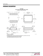
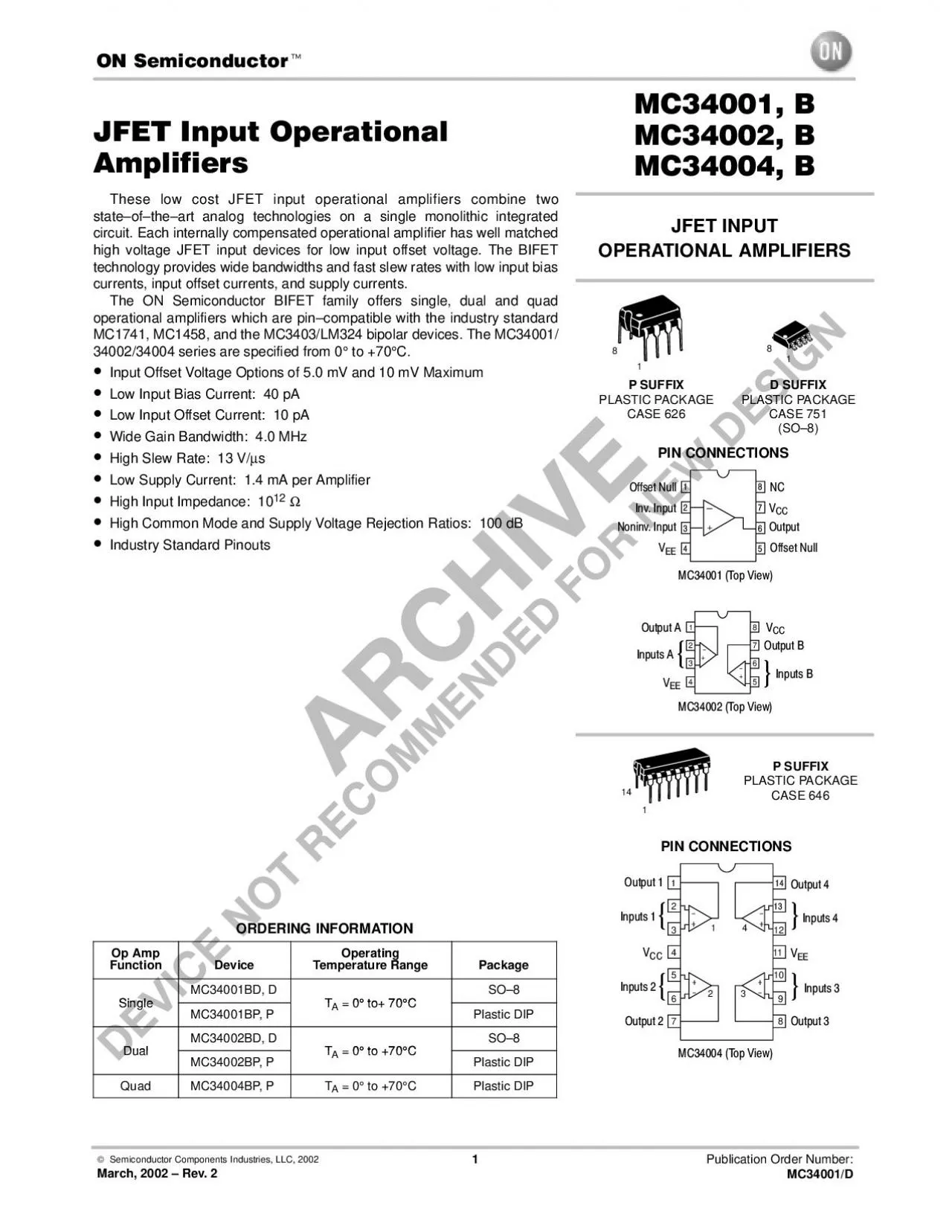
/
These low cost JFET input operational amplifiers combine twostate±of These low cost JFET input operational amplifiers combine twostate±of

These low cost JFET input operational amplifiers combine twostate±of - PDF document

jalin
jalin . @jalin
Follow
343 views
Uploaded On 2021-01-05

These low cost JFET input operational amplifiers combine twostate±of - PPT Presentation

Device Temperature Range Single to70 Single MC34001BP P TA to 705C to70 Dual MC34002BP P TA to 705C MC34004BP P TA to 705C 1 March 2002 Rev 2 MC34001 BJFET INPUTOPERATIONAL AMPLIFIERS ID: 828212

input voltage supply mc34001 voltage input mc34001 supply mc34002 mc34004 output temperature offset 100 current swing dimension ambient http

Share:

Link:

Embed:

Download Presentation from below link

Download Pdf The PPT/PDF document "These low cost JFET input operational am..." is the property of its rightful owner. Permission is granted to download and print the materials on this web site for personal, non-commercial use only, and to display it on your personal computer provided you do not modify the materials and that you retain all copyright notices contained in the materials. By downloading content from our website, you accept the terms of this agreement.


Presentation Transcript

These low cost JFET input operational am
These low cost JFET input operational amplifiers combine twostate±of±the±art analog technologies on a single monolithic integratedhigh voltage JFET input devices for low input offset voltage. The BIFETcurrents, input offset currents, and supply currents.The ON Semiconductor BIFET family offers single, dual and quadoperational amplifiers which are pin±compatible with the industry standard34002/34004 series are specified from 0to+70Input Offset Voltage Options of 5.0 mV and 10 mV MaximumLow Input Bias Current:40 pALow Input Offset Current:10 pAWide Gain Bandwidth:4.0 MHzHigh Slew Rate:13 V/Low Supply Current:1.4 mA per AmplifierHigh Input Impedance:10High

Common Mode and Supply Voltage Rejectio
Common Mode and Supply Voltage Rejection Ratios:100 dBORDERING INFORMATIONDeviceTemperature RangeSingleto+70SingleMC34001BP, PTA to+ 705Cto+70DualMC34002BP, PTA to +705CMC34004BP, PTA to +705CMarch, 2002 ± Rev. 2MC34001, BJFET INPUTOPERATIONAL AMPLIFIERSOffset NullPLASTIC PACKAGEPLASTIC PACKAGEMC34001 (Top View)PIN CONNECTIONSMC34002 (Top View)Offset NullNoninv. InputInv. InputOutput A V1234875+-++12348765188PLASTIC PACKAGEPIN CONNECTIONSInputs 1MC34004 (Top View)-12346101314+-++-+-141MC34001, B MC34002, B MC34004, BMAXIMUM RATINGSSymbolValueUnitSupply VoltageV18VDifferential Input Voltage (Note 1)30VInput Voltage R

angeV16VOperating Ambient Temperatur
angeV16VOperating Ambient Temperature RangeACOperating Junction TemperatureTJ1505CStorage Temperature RangeC1.Unless otherwise specified, the absolute maximum negative input voltage is equal to thenegative power supply.ELECTRICAL CHARACTERISTICS = +15 V, V = ±15 V, TSymbolMinTypUnitInput Offset Voltage (RV3.05.010mVAverage Temperature Coefficient of Input Offset VoltageVDTÐ10ÐmV/5CInput Offset Current (VI25100pAMC3400XI50200pAiÐ10WCommon Mode Input Voltage Range+15±12ÐVLarge Signal Voltage Gain (V10 V, RVOL150ÐV/mVOutput Voltage SwingO+12+10+14+13ÐÐV 3MC3400XCMRR80100ÐdBSupply Voltag

e Rejection Ratio (RPSRR80100ÐdBM
e Rejection Ratio (RPSRR80100ÐdBMC3400XIDÐ1.42.5mAÐ13ÐV/msÐ4.0ÐMHzEquivalent Input Noise VoltagenÐ25ÐnV/HznÐ0.01ÐpA/Hz2.TC for MC34001/34001BT=+703.The input bias currents approximately double for every 104.Supply voltage rejection ratio is measured for both supply magnitudes increasing or decreasing simultaneously, in accordance MC34001, B MC34002, B MC34004, BELECTRICAL CHARACTERISTICS = +15 V, V = ±15 V, TSymbolMinTypUnitInput Offset Voltage (RVÐ7.013mVInput Offset Current (VIÐ4.0nAMC3400XIÐ8.0nACommon Mode Input Voltage RangeÐV10 V, RVOLÐÐV/mVOutput Voltage SwingO+12+10ÐÃ

ÃV 3MC3400XCMRR80ÐÐdBSupply
ÃV 3MC3400XCMRR80ÐÐdBSupply Voltage Rejection Ratio (RPSRR80ÐÐdBMC3400XIDÐÐ2.8mA2.TC for MC34001/34001BT=+703.The input bias currents approximately double for every 104.Supply voltage rejection ratio is measured for both supply magnitudes increasing or decreasing simultaneously, in accordance MC34001, B MC34002, B MC34004, Bhttp://onsemi.com4+LL+LAC, OUTPUT VOLTAGE SWING (V, OUTPUT VOLTAGE SWING (V, OUTPUT VOLTAGE SWING (Vversus TemperatureFigure 2. Output Voltage SwingFigure 3. Output Voltage SwingFigure 4. Output Voltage Swingversus Supply VoltageFigure 5. Output Voltage Swingversus Temperatureversus Temperature, AMBIE

NT TEMPERATURE (-75-50-2502550751001251
NT TEMPERATURE (-75-50-2502550751001251001.0 k10 k100 k1.0 M10 M, LOAD RESISTANCE (k0.10.20.40.71.02.010 , SUPPLY VOLTAGE (V)05.0101520, AMBIENT TEMPERATURE (-50-250255075100125, AMBIENT TEMPERATURE (-50-250255075100125I, SUPPLY DRAIN CURRENT (mA)OUTPUT VOLTAGE SWING (V, INPUT BIAS CURRENT (nA)MC34001, B MC34002, B MC34004, Bhttp://onsemi.com5Figure 7. Large±Signal Voltage Gain andFigure 8. Large±Signal Voltage Gainversus Temperatureversus TemperatureFigure 10. Equivalent Input Noise VoltageFigure 11. Total Harmonic DistortionPHASE SHIFT (DEGREES)1.0101001.0 k10 k100 k1.0 M1.0 M10 MVOL+LACA, VOLTAGE GAIN (V/mV)

, AMBIENT TEMPERATURE (-50-250255075100
, AMBIENT TEMPERATURE (-50-250255075100125, AMBIENT TEMPERATURE (NORMALIZED SLEW RATE-50-2502550751001250.010.050.10.51.05.01050100+VSTACTHD, TOTAL HARMONIC DISTORTION (%)0.10.51.05.01050100nV/Hz ), OPEN-LOOP GAIN, EQUIVALENT INPUT NOISE VOLTAGE (60504030201001.00.50.10.050.010.0050.0010545590513551805MC34001, B MC34002, B MC34004, Bhttp://onsemi.com6Figure 12. Output Current to Voltage TransformationQ4Q5J1J22.0 kQ11OffsetR2VVs The value of C may be selected to minimize overshootand ringing.Theoretical VVO(RO)A1A2A3A4A5A6A7A8248163264128256+++++++oMC34001, B MC34002, B MC34004, BFigure 14. Long Interval RC TimerFigure 15. Isolating Large

Capacitive LoadsFigure 16. Wide BW, Low
Capacitive LoadsFigure 16. Wide BW, Low Noise,maxPower BW: fmaxTo compensate add C2 such that: R2C2 0.5L =OV7643MC34001VLLFCC DVO IV/mt-+O(max)V23-+65-+7ResetVin4VMC340021N914F*ResetNetwork*Polycarbonate capacitorD1 = Hi-speed, low-reverse leakage diodeOMC34001R1V1R3Time (t) = R4 Cn (VDesign Example: 100 Second TimerMC34002MC34001, B MC34002, B MC34004, BPLASTIC PACKAGEPLASTIC PACKAGE1.DIMENSION L TO CENTER OF LEAD WHENFORMED PARALLEL.2.PACKAGE CONTOUR OPTIONAL (ROUND OR3.DIMENSIONING AND TOLERANCING PER ANSI8FNOTE 2SEATINGLMMA0.13 (0.005)BMTDIMMINMAXMINMAXA9.4010.160.3700.4006.106.600.2400.2603.944.450.1550.1750.380.510.01

50.0201.021.780.0400.0702.54 BSC0.100 BS
50.0201.021.780.0400.0702.54 BSC0.100 BSC0.761.270.0300.0500.200.300.0080.0122.923.430.1150.1357.62 BSC0.300 BSC---10 ---10 0.761.010.0300.040SEATINGA0.25MMBMhCX 45LDIMMINMAXA1.351.750.100.250.350.490.180.254.805.003.804.005.806.200 7 0.401.250.250.501.DIMENSIONING AND TOLERANCING PER ASME2.DIMENSIONS ARE IN MILLIMETERS.3.DIMENSION D AND E DO NOT INCLUDE MOLD4.MAXIMUM MOLD PROTRUSION 0.15 PER SIDE.5.DIMENSION B DOES NOT INCLUDE MOLDPROTRUSION. ALLOWABLE DAMBARPROTRUSION SHALL BE 0.127 TOTAL IN EXCESSOF THE B DIMENSION AT MAXIMUM MATERIALDEHBA1A0.10MC34001, B MC34002, B MC34004, BPLASTIC PACKAGE1.LEADS WITHIN 0.13 (0.005) RADIUS

OF TRUEPOSITION AT SEATING PLANE AT MAXI
OF TRUEPOSITION AT SEATING PLANE AT MAXIMUMMATERIAL CONDITION.2.DIMENSION L TO CENTER OF LEADS WHENFORMED PARALLEL.3.DIMENSION B DOES NOT INCLUDE MOLD4.ROUNDED CORNERS OPTIONAL.148HGDSEATINGDIMMINMAXMINMAX0.7150.77018.1619.560.2400.2606.106.600.1450.1853.694.690.0150.0210.380.530.0400.0701.021.780.100 BSC2.54 BSC0.0520.0951.322.410.0080.0150.200.380.1150.1352.923.430.300 BSC7.62 BSC0 10 0 10 0.0150.0390.391.01MC34001, B MC34002, B MC34004, Bhttp://onsemi.com10NOTESMC34001, B MC34002, B MC34004, Bhttp://onsemi.comMC34001, B MC34002, B MC34004, Bhttp://onsemi.com12ON Semiconductorto make changes without further notice to any produ

cts herein. SCILLC makes no warranty, r
cts herein. SCILLC makes no warranty, representation or guarantee regardingand all liability, including without limitation special, consequential or incidental damages. ªTypicalº parameters which may band/or ferent applications and actual performance may vary over time. All operating parameters, including ªTypicalsº mustbe validated for each customer application by customer's technical experts. SCILLC does not convey any license under its patenSCILLC may occur. Should Buyer purchase or use SCILLC products for any such unintended or unauthorized application, Buyer shall indemand its officers, employees, subsidiaries, affiliates, and distributors har

mless against all claims, costs, damages
mless against all claims, costs, damages, and expenses, and rearising out of, directly or indirectly, any claim of personal injury or death associated with such unintended or unauthorized uSCILLC was negligent regarding the design or manufacture of the part. SCILLC is an Equal Opportunity/Affirmative Action Employer.PUBLICATION ORDERING INFORMATIONJAPAN: ON Semiconductor, Japan Customer Focus Center4±32±1 Nishi±Gotanda, Shinagawa±ku, Tokyo, Japan 141±0031ON Semiconductor WebsiteP.O. Box 5163, Denver, Colorado 80217 USA: 303±675±2175 or 800±344±3860 Toll Free USA/CanadaToll Free USA/CanadaN. American Technical Support: 800±282±9855 Toll Free US