/
Analog Applications Journal Texas Instruments Incorporated Q  www Analog Applications Journal Texas Instruments Incorporated Q  www

Analog Applications Journal Texas Instruments Incorporated Q www - PDF document

luanne-stotts
luanne-stotts . @luanne-stotts
Follow
473 views
Uploaded On 2014-12-24

Analog Applications Journal Texas Instruments Incorporated Q www - PPT Presentation

ticomaaj HighPerformance Analog Products Using fully differential op amps as attenuators Part 1 Differential bipolar input signals Introduction Conditioning highvoltage input signals to drive ADCs from highvoltage sources can be challenging How can a ID: 28730

ticomaaj HighPerformance Analog Products Using

Share:

Link:

Embed:

Download Presentation from below link

Download Pdf The PPT/PDF document "Analog Applications Journal Texas Instru..." is the property of its rightful owner. Permission is granted to download and print the materials on this web site for personal, non-commercial use only, and to display it on your personal computer provided you do not modify the materials and that you retain all copyright notices contained in the materials. By downloading content from our website, you accept the terms of this agreement.


Presentation Transcript

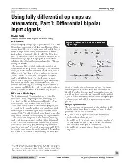
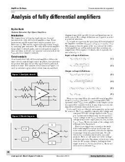
Analog Applications JournalTexas Instruments Incorporated 2Q 2009www.ti.com/aajHigh-Performance Analog ProductsUsing fully differential op amps as attenuators, Part 1: Differential bipolar input signalsConditioning high-voltage input signals to drive ADCs from high-voltage sources can be challenging. How can a higher-voltage signal like ±10 V be attenuated and level-shifted to match the significantly lower differential and common-mode-voltage input required by the ADC? In this article, Noise gain is used to define the stability criteria of an op amp and is calculated S– ++––FDA Figure 1. Attenuator circuit for differential bipolar input Texas Instruments Incorporated Analog Applications Journal High-Performance Analog Products www.ti.com/aaj 2Q 2009Op AmpsFor analysis, it is convenient to assume that the FDA is an ideal amplifier with no offset and has infinite gain. The first step in analyzing the circuit in Figure 1 is to simplify it by using only its attenuator portion and the Thevenin equivalent of the input source. This is shown in Figure 2. With the circuit in this form, it is easier to see that its overall gain can be calculated by the formula VVRRRRRRROUTSigTSTFGST222. The noise gain of the FDA can be set to 2 by making the second half of Equation 1 equal to 1: RRRRGSTF22 With this constraint, the overall gain equation reduces to VVRRROUTSigTST2. There are two degrees of freedom for choosing components in the gain equation—an infinite number of combinations of R and R that will give the desired input attenuation, and an infinite number of R and R values to set the gain.The differential input impedance of this amplifier circuit is given by Z = 2R + R || 2R. Depending on the attenuation needed, the input impedance is approximately 2RIt is recommended that R be kept to a range of values for the best performance. Too large a resistance will add excessive noise and will possibly interact with parasitic board capacitance to reduce the bandwidth of the ampli - fier; and too low a resistance will load the output, causing increased distortion. Design is best accomplished by first choosing R close to the desired input impedance, then choosing R within the recommended range for the device. For example, the THS4521 performs best with R at about 1 k. Next, the value of R required to give the desired attenuation is calculated. Then R is calculated for the desired gain. These equations are easily solved when set up in a spreadsheet. To see an example Excel worksheet, go to http://www.ti.com/lit/zip/slyt336 and click Open to view the WinZip directory online (or click Save to download the WinZip file for offline use). Then open the file FDA_Attenuator_Examples_Diff_Bipolar_Input.xls and select the Diff Bipolar FDA Input Atten worksheet tab.Design Example 1As a design example, let’s say we have a 20-V differential bipolar (±10-V) signal, and we need a 2-k differential input impedance. We want to use the ADS8321 SAR ADC with a 5-V differential input and a 2.5-V common-mode voltage. We choose R = 1 k and R = 1 k. Rearranging Equation 3 and using substitution, we can calculate The nearest standard 1% value, 665 , should be used. Then, rearranging Equation 2 and using substitution, we can calculate which is a standard 1% value. These values will provide e needed attenuation function and will keep the FDA stable. The V input on the FDA is then used to set the output common-mode voltage to 2.5 V.The input impedance is which is higher than desired. If the input impedance really be closer to 2 k, we can iterate with a lower value. In this case, using R = 806 and R = 1 k will yield Z = 2014 , which comes as close as is possible when standard 1% values are used.SPICE simulation is a great way to validate the design. To see a TINA-TI™ simulation of the circuit in Example 1, Figure 2. Thevenin-equivalent input source and attenuator VRRRSigTST2 22RRST 22RRST Texas Instruments Incorporated Analog Applications Journal 2Q 2009www.ti.com/aajHigh-Performance Analog ProductsAmplifiers: Op Ampsgo to http://www.ti.com/lit/zip/slyt336 and click Open to view the WinZip directory online (or click Save to download the WinZip file for offline use). If you have the TINA-TI software installed, you can open the file FDA_Attenuator_Examples_Diff_Bipolar_Input.TSC to view the example (the top circuit labeled “Example 1”). To download and install the free TINA-TI software, visit www.ti.com/tina-ti and click the Download button.The simulation waveforms in Figure 3 show that the circuit simulates as expected. V is the 20-V input; is the differential output of the amplifier circuit; and V and V are the individual outputs of the amplifier.Using an FDA’s RThe proposed circuit using gain-setting resistors to obtain a balanced, differential bipolar input signal is shown in Figure 4. In this circuit, the FDA is used as an attenuator in a manner similar to using an inverting op amp. The gain (or attenuation) is set by R and R VVRROUTSigFG is used to set the noise gain to 2 for stability: RRRFGT2 The equation for input impedance is Z = 2RDesign Example 2Using the same approach as for Example 1, with R = 1 kwe calculate R = 4 k (the nearest standard 1% value is 4.02 k) and R = 2.67 k (a standard 1% value). This makes Z = 8.04 k. The simulation results are the same as before, but with this approach the only freedom of choice given the design requirements is the value of R Time (µs)00.51.01.52.0 Figure 3. TINA-TI simulation waveforms of differential bipolar input in Example 1 VS+VS–RFRFRGRTRGVSigVOUT–VOUT+VOCM ++––FDA Figure 4. Using FDA’s R Texas Instruments Incorporated Analog Applications Journal High-Performance Analog Products www.ti.com/aaj 2Q 2009Amplifiers: Op To see an example Excel worksheet, go to http://www.ti.com/lit/zip/slyt336 and click Open to view the WinZipdirectory online (or click Save to download the WinZip file for offline use). Then open the file FDA_Attenuator_Examples_Diff_Bipolar_Input.xls and select the Diff Bipolar FDA Rf_Rg Atten worksheet tab. To see a TINA-TI simulation of the circuit in Example 2, go to http://www.ti.com/lit/zip/slyt336 and click Open to view the WinZip directory online (or click Save to download the WinZip file for offline use). If you have the TINA-TI software installed, you can open the file FDA_Attenuator_Examples_Diff_Bipolar_Input.TSC to view the example (the bottom circuit labeled “Example 2”). Note that this circuit provides the same results as for the circuit in Example 1. To download and install the free TINA-TI software, visit www.ti.com/tina-ti and click the Download button.We have analyzed two approaches that attenuate and level-shift high-amplitude, differential bipolar signals to the input range of lower-voltage input ADCs. The first approach uses an input attenuator with values chosen to provide the required attenuation and to keep the noise gain of the FDA equal to 2 for stability. The second approach uses the gain-setting resistors of the FDA in much the same way as using an inverting op amp, then a resistor is bootstrapped across the inputs to provide a noise gain of 2. The two approaches yield the same voltage translation that is needed to accomplish the interface task. Other performance metrics were not analyzed here, but the two approaches have substantially the same noise, bandwidth, and other AC and DC performance characteristics as long as the value of R is the same.The input-attenuator approach shown in Example 1 is more complex but allows the input impedance to be adjusted independently of the gain-setting resistors used around the FDA. At least to a certain degree, lower values can easily be achieved if desired, but there is a maximum allowable R where larger values require the R resistor to be a negative value. For example, setting R = 4 k results in R = 0 . The spreadsheet tool provided will generate “#NUM!” errors for this input as it tries to calculate the nearest standard value, which then replicates throughout the rest of the cells that require a value for R; but this value will work.It should be noted that a circuit similar to the one in Example 1, with a maximum R value and R = 0 results in the same circuit as the one in Example 2 that uses the gain-setting resistors as the attenuator. It should also be noted that the source impedance will affect the input gain or attenuation of either circuit and should be included in the value of R, especially if it is significant.The approach in Example 2 is easier, but the input impedance is set as a multiplication of the feedback resistor and attenuation: Z = 2 x R x Attenuation. This does allow some design flexibility by varying the value of Rbut the impact on noise, bandwidth, distortion, and other performance characteristics should be considered.For more information related to this article, you can down - load an Acrobat Reader file at www-s.ti.com/sc/techlit/ and replace “” with the TI Lit. # for the materials listed below.Document Title TI Lit. # Jim Karki, “Fully-Differential Amplifiers,” Application Report ........................ Related Web sitesamplifier.ti.comwww.ti.com/sc/device/ADS8321www.ti.com/sc/device/THS4521TINA-TI and spreadsheet support files for examples:www.ti.com/lit/zip/slyt336To download TINA-TI software:www.ti.com/tina-ti IMPORTANT NOTICE Texas Instruments Incorporated and its subsidiaries (TI) reserve the right to make corrections, modifications, enhancements, improvements, and other changes to its products and services at any time and to discontinue any product or service without notice. Customers should obtain the latest relevant information before placing orders and should verify that such information is current and complete. All products are sold subject to TIs terms and conditions of sale supplied at the time of order acknowledgment. TI warrants performance of its hardware products to the specifications applicable at the time of sale in accordance with TI's standard warranty. Testing and other quality control techniques are used to the extent TI deems necessary to support this warranty. Except where mandated by government requirements, testing of all parameters of each product is not necessarily performed. TI assumes no liability for applications assistance or customer product design. Customers are responsible for their products and applications using TI components. To minimize the risks associated with customer products and applications, customers should provide adequate design and operating safeguards. TI does not warrant or represent that any license, either express or implied, is granted under any TI patent right, copyright, mask work right, or other TI intellectual property right relating to any combination, machine, or process in which TI products or services are used. Information published by TI regarding third-party products or services does not constitute a license from TI to use such products or services or a warranty or endorsement thereof. Use of such information may require a license from a third party under the patents or other intellectual property of the third party, or a license from TI under the patents or other intellectual property of TI. Reproduction of information in TI data books or data sheets is permissible only if reproduction is without alteration and is accompanied by all associated warranties, conditions, limitations, and notices. Reproduction of this information with alteration is an unfair and deceptive business practice. TI is not responsible or liable for such altered documentation. Information of third parties may be subject to additional restrictions. Resale of TI products or services with statements different from or beyond the parameters stated by TI for that product or service voids all express and any implied warranties for the associated TI product or service and is an unfair and deceptive business practice. TI is not responsible or liable for any such statements. TI products are not authorized for use in safety-critical applications (such as life support) where a failure of the TI product would reasonably be expected to cause severe personal injury or death, unless officers of the parties have executed an agreement specifically governing such use. Buyers represent that they have all necessary expertise in the safety and regulatory ramifications of their applications, and acknowledge and agree that they are solely responsible for all legal, regulatory and safety-related requirements concerning their products and any use of TI products in such safety-critical applications, notwithstanding any applications-related information or support that may be provided by TI. Further, Buyers must fully indemnify TI and its representatives against any damages arising out of the use of TI products in such safety-critical applications. TI products are neither designed nor intended for use in military/aerospace applications or environments unless the TI products are specifically designated by TI as military-grade or enhanced plastic. Only products designated by TI as military-grade meet military specifications. Buyers acknowledge and agree that any such use of TI products which TI has not designated as military-grade is solely at the Buyer's risk, and that they are solely responsible for compliance with all legal and regulatory requirements in connection with such use. TI products are neither designed nor intended for use in automotive applications or environments unless the specific TI products are designated by TI as compliant with ISO/TS 16949 requirements. Buyers acknowledge and agree that, if they use any non-designated products in automotive applications, TI will not be responsible for any failure to meet such requirements. Following are URLs where you can obtain information on other Texas Instruments products and application solutions: Products amplifier.ti.com Data Converters dataconverter.ti.com Productswww.dlp.comClocks and Timerswww.ti.com/clocksPower Mgmt power.ti.com Microcontrollers microcontroller.ti.com www.ti-rfid.comRF/IF and ZigBeewww.ti.com/lprf Solutionswww.ti.com/audio www.ti.com/automotive Broadband www.ti.com/broadband Digital Control www.ti.com/digitalcontrol www.ti.com/medicalwww.ti.com/military Optical Networking www.ti.com/opticalnetwork www.ti.com/security Telephony www.ti.com/telephony Video & Imaging www.ti.com/video Wireless www.ti.com/wirelessMailing Address: Texas Instruments Post Office Box 655303 Dallas, Texas 75265 TI Worldwide Technical Support PageTI Semiconductor KnowledgeBase Home PageMexicoEurope, Middle East, and Africa The European Free Call (Toll Free) number is not active in all countries. If you have technical difficulty calling the free call number, www.tij.co.jp/pic Toll-Free Number Taiwan © 2009 Texas Instruments IncorporatedTINA-TI is a trademark of Texas Instruments. Acrobat and Reader are registered trademarks of Adobe Systems Incorporated. Excel is a registered trademark of Microsoft Corporation. WinZip is a registered trademark of WinZip International LLC. All other trademarks are the property of their respective owners.Safe Harbor Statement: This publication may contain forward-looking statements that involve a number of risks and uncertainties. These “forward-looking statements” are intended to qualify for the safe harbor from liability established by the Private Securities Litigation Reform Act of 1995. These forward-looking statements generally can be identified by phrases such as TI or its management “believes,” “expects,” “anticipates,” “foresees,” “forecasts,” “estimates” or other words or phrases of similar import. Similarly, such statements herein that describe the company's products, business strategy, outlook, objectives, plans, intentions or goals also are forward-looking statements. All such forward-looking statements are subject to certain risks and uncertainties that could cause actual results to differ materially from those in forward-looking statements. Please refer to TI's most recent Form 10-K for more information on the risks and uncertainties that could materially affect future results of operations. We disclaim any intention or obligation to update any forward-looking statements as a result of developments occurring after the date SLYT336