/
MT TUTORIAL Aperture Time Aperture Ji tter Aperture Delay Time Removing the Confusion MT TUTORIAL Aperture Time Aperture Ji tter Aperture Delay Time Removing the Confusion

MT TUTORIAL Aperture Time Aperture Ji tter Aperture Delay Time Removing the Confusion - PDF document

pasty-toler
pasty-toler . @pasty-toler
Follow
533 views
Uploaded On 2015-02-17

MT TUTORIAL Aperture Time Aperture Ji tter Aperture Delay Time Removing the Confusion - PPT Presentation

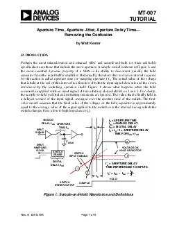
A simple model is shown in Figure 1 and the most essential dynamic property of a SHA is its ability to disconnect quickly the hold capacitor from the input buffer amplifier Historical ly the short but nonzero interval required for this action is cal ID: 36025

simple model

Share:

Link:

Embed:

Download Presentation from below link

Download Pdf The PPT/PDF document "MT TUTORIAL Aperture Time Aperture Ji tt..." is the property of its rightful owner. Permission is granted to download and print the materials on this web site for personal, non-commercial use only, and to display it on your personal computer provided you do not modify the materials and that you retain all copyright notices contained in the materials. By downloading content from our website, you accept the terms of this agreement.


Presentation Transcript

tter, Aperture Delay Time— by Walt Kester Perhaps the most misunderstood and misused ADC and sample-and-hold (or track-and-hold) specifications are those that include the word . A simple model is shown in Figure 1, and the most essential dynamic property of a SHA is its ability to disconnect quickly the hold capacitor from the input buffer amplifier. Historicalfor this action is called aperture time (or sampling aperture)command is applied with an input signal of two arthe sample-to-hold pedestal and switching transients are ignored. The value that is finally held is over the aperture time 1 2 2ta SAMPLEHOLD SWITCHDRIVER ANALOGDELAY, DIGITALDELAY, APERTURETIME, VOLTAGE ONHOLD CAPACITOR SWITCHDRIVER OUTPUT = APERTURE TIME= ANALOG DELAY= DIGITAL DELAY ' = APERTURE DELAYTIME REFERENCED TO INPUTS ta2 HOLD Figure 1: Sample-and-Hold Waveforms and Definitions Rev.A, 10/08, WK Page 1 of 8 MT-007 The model shows that the finite time required for the switch to open (t) is equivalent to introducing a small delay t in the sampling clock driving the can be either positive or negative. The diagram shows that the same value of t works for the two , or simply In an ADC, the aperture delay time is referenced to the input of the converter, and the effects of , must be considered. Referenced to the ADC inputs, aperture time, t', is defined as the time difference between the analog pr, plus one-half the aperture time, tThe effective aperture delay time is usually positive, but may be negative if the sum of one-half the aperture time, t/2, and the switch driver digital delay, tthrough the input buffer, tthus establishes when the input signal is actually sampled with respect to the sampling clock edge. Aperture delay time can be measured by appladjusting the synchronous sampling clock delay such that the output of the ADC is mid-scale sampling clock edge and the actual zero-crossing of the input sinewave is the aperture delay time SAMPLINGCLOCKANALOG INPUTSINEWAVEZERO CROSSING+FS ''' Measured with Respect to ADC Input Page 2 of 8 MT-007 (assuming it is relatively short with respect to the hold time), but acts as a fixed delay in either the samplisign). However, in "interleaved" ADCs, simultaneous sampling applicationsdemodulation, where two or more ADCs must be well matched; variations between converters can produce errors on fast slewlications, the aperture delay mismatches must be removed by properly adjusting the phases of the individual sampling ), then a in the instant the switch opens is called aperture uncertaintymeasured in rms picoseconds. The amplitude of the associated output error is related to the rate-of-chincreases. The effects of phase jitter on the external sampling clock (or the analog input for that matter) produce exactly the same type of error. For this reason, the total amount of jitter is the root-sum-square of the external sampling cl ANALOGINPUTTRACKHOLD dvdtv dvdt RMS= APERTURE JITTERRMSNOMINALOUTPUT = SLOPE = APERTURE JITTER ERROR Figure 3: Effects of Aperture Jitter and Sampling Clock Jitter Page 3 of 8 MT-007 SIGNAL-TO-NOISE RATIO (SNR) The effects of aperture and sampling clock jittfollowing simple analysis. Assume an input signal given by ft. Eq. 1 ft2cosVf2π=. Eq. 2 The rms value of dv/dt can be obtained by dividing the amplitude, 2, by fV2. Eq. 3 rmst = the rms aperture jitter t, and substitute these fV2 . Eq. 4 rms tfV2jO =Δ. Eq. 5 The rms value of the full-scale input sinewave is V2, therefore the rms signal to rms noise jOtf2log202/tfV22/Vlog202/Vlog20SNR. Eq. 6 This equation assumes an infinite resolution ADC where aperture jitter is the only factor in determining the SNR. This equation is plotted aperture and sampling clock jitter on SNR and ENOB, especially atve 14-bit SNR performance when sampling a 100-MHz IF signal, the aperture jitter must be less than 0.1 ps. ADCs are currently available with typical aperture jitter specifications of 60-fs rms ( 14-bits @ 125 MSPS and AD9446 16-bits @ 100 MSPS). Extreme care must be taken to minimize phase noise in the sampling/reconstruction clock so asrformance of the ADC itself. Page 4 of 8 MT-007 (dB)ENOB 10030100= 100ps= 10ps= 1ps = 0.1ps 120 FULL-SCALE SINEWAVE ANALOG INPUT FREQUENCY (MHz)SNR = 20log SNR = 20log = 50fs This care must extend to all aspects of the clock sitimer is absolutely inadequate, but even a quartz crproblems if it uses an active device which shares a chip with noisy logic); the transmission path (these clocks are very vulnerable to interference of all sorts), and phase noise introduced in the ADC or DAC. As integral sample-and-hold (SHA) circuitry, however the total rms jitter will be composed of a number of components—the actubeing the least of them. Before the 1980s, most sampling ADCs were generally built from a separate SHA and ADC. Interface design was complex, and accurately predicting the performance of the combination was difficult. Today, almost all sampled data systems use ADCs which contain an integral SHA. The aperture jitter of the SHA may not be specified as such, but this is not a cause of since a guarantee of a specific SNR at a specific input frequency is an implicte aperture jitter specification. Page 5 of 8 MT-007 MEASURING ADC APERTURE JITTER USING FFT TECHNIQUES The FFT test routine for measuring ADC SNR, SFDR, etc., is an excellent indirect method for measuring aperture jitter. The caveat in this test is that the measurement includes the jitter of the sampling clock generator as well as the ADC internal aperture jitter. should be selected with an rms jitter specification which is several times less than the specified the ADC under test, since individual jitter components combine on an rss basis. The basic test setup for the aperture jitter test is shown in Figure 5 along with the key calculations. ADC SINEWAVESIGNALGENERATOR LOW JITTER CLOCKGENERATOR M-WORDMEMORY(FIFO) N PC PARALLEL, SERIAL, ORUSB INTERFACE SNR FOR LOW FREQUENCY FS INPUT = SNRL SNR FOR HIGH FREQUENCY FS INPUT = SNRH (FREQUENCY = f)SNRA = 20 log 2fta ta= 1 –SNRH/20 –SNRL/20 2– INCLUDES JITTER OF CLOCK GENERATOR Figure 5: Measuring Aperture Jitter Based on There are two SNR measurements required, and bot. The first measurement, SNRL, is madewhere the noise is primarily the combinatimeasure the same SNR value. The sampling frset for the maximum allowable. The second measurement, SNRH, , where the effects of aperture jitter on the ADC SNR are noticeable. Depending on the ADC, this frequency may be as high as ftween the signal-to-noise ratio due to aHtf2log20SNRA, Eq. 7 where SNRA is the SNR (dB) due to aperture jitter, and f Page 6 of 8 MT-007 Solving for t 20/SNRAf2. Eq. 8 procals can then be combined on an rss basis: 20/SNRA20/SNRL20/SNRH. Eq. 9 20/SNRL20/SNRH20/SNRA. Eq. 10 Substituting Eq. 10 into Eq. 8: 20/SNRL20/SNRHf2. Eq. 11 It should be emphasized that all the measurements required for is extremely important that the 2harmonics (as well as the dc components) be removed when making the SNR calculation from the FFT output. Otherwise, the measurement will not give an accurate measure As a final note, measuring rms aperture jitter less than 10-ps rms is extremely difficult, simply because of unwanted jitter which may occur on ADC sampling clock, or layout-induced jitter and noise. Obtaining this le Page 7 of 8 Page 8 of 8 REFERENCES: Brad Brannon, "Aperture Uncertainty and ADC System Performance Application Note, Analog Devices, Inc., January 1998. (available for download at http://www.analog.com) Hank Zumbahlen, Basic Linear Design, Analog Devices, 2006, ISBN: 0-915550-28-1. Also available as Linear Circuit Design Handbook , Elsevier-Newnes, 2008, ISBN-10: 0750687037, ISBN-13: 978-0750687034. Analog-Digital Conversion , Analog Devices, 2004, ISBN 0-916550-27-3, Chapters 2 and 5. Also available as The Data Conversion Handbook Elsevier/Newnes, 2005, ISBN 0-7506-7841-0, Chapters 2 and 5.Copyright 2009, Analog Devices, Inc. All rights reserved. Analog Devices assumes no responsibility for customer product design or the use or application of customers’ products or for any infringements of patents or rights of others which may result from Analog Devices assistance. All trademarks and logos are property of their respective holders. Information furnished by Analog Devices applications and development tools engineers is believed to be accurate and reliable, however no responsibility is assumed by Analog Devices regarding technical accuracy and topicality of the content provided in Analog Devices Tutorials.