Explore
Featured
Recent
Articles
Topics
Login
Upload
Featured
Recent
Articles
Topics
Login
Upload
Search Results for 'Wafer-Thickness'
Wafer-Thickness published presentations and documents on DocSlides.
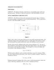
THICKNESS MEASUREMENTTHICKNESS The distance through a wafer between corresponding points on the frontand back surface. Thickness is expressed in microns or mils (thousandths of an inch).TOTAL THICKNESS VARIATION (TTV) The difference between the maximum
by karlyn-bohler
B WAFER w G MEASUREMENT AXIS PROBE A PROBE B A Fig...
Silicon wafers Microchips are made on silicon wafers.
by calandra-battersby
Silicon wafer. www.guardian.co.uk. http://. mrsec...
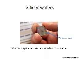
Silicon wafers Microchips are made on silicon wafers.
by faustina-dinatale
Silicon wafer. www.guardian.co.uk. http://. mrsec...
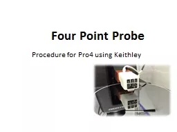
Four Point Probe Procedure for Pro4 using Keithley
by conchita-marotz
Overview. What is Four Point Probing. How the sys...
Creating Snow flake structures
by alexa-scheidler
using EBL. Date:. January 2011. by:. Lejmarc. Sn...
Hazelnut Coffee/Wafers
by celsa-spraggs
By Taylor . Vesel. Hazelnut Coffee, a flavor for ...
Hazelnut Coffee/Wafers
by natalia-silvester
By Taylor . Vesel. Hazelnut Coffee, a flavor for ...
Silicon Wafer Committee Europe
by mitsue-stanley
Werner Bergholz, Jacobs University Bremen. Friedr...
ABC130 Wafer Probe
by test
Peter W Phillips. 12/03/2014. ABC130 Wafer Probe....
Sensor and Assembly status
by leah
Mathieu Benoit . CNM . Sensor. Production. As of ...
THICKNESS MEASUREMENTTHICKNESS The distance through a wafer between c
by trish-goza
B WAFER w G MEASUREMENT AXIS PROBE A PROBE B A Fig...
Four Point Probe
by tatiana-dople
Procedure for Pro4 using Keithley. Overview. What...
Split thickness flap/ mucosal flap
by barbara
Full thickness . mucoperiosteal. flap. Using surg...
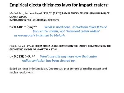
Empirical ejecta thickness laws for impact craters:
by hanah
McGetchin. , Settle & Head EPSL 20 (1973) . RA...
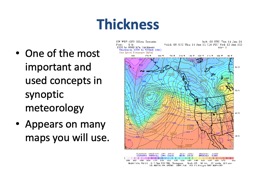
Thickness One of the most important and used concepts in synoptic meteorology
by piper
Appears on many maps you will use.. Thickness. is...
Breast Thickness and Lesion Depth Measurement28J HK Coll Radiol 20036
by madison
J HK Coll Radiol 2003;6:28-29 TECHNICAL NOTE Small...
Cartilage Stiffness and Thickness Distributions Revealed by an Automated Indentation Technique in t
by LovableLatina
TMJ Bioengineering Conference. Barcelona, Spain. S...
Can we apply topological methods to cortical thickness data?
by susan
Topological methods and cortical thickness. Chung ...
Using Fractional Lake Ice and Variable Ice Thickness in the
by faustina-dinatale
Michael . Dutter. and Todd . Kluber. NOAA/Nation...
Cortical Thickness Analysis with Slicer
by alida-meadow
Martin Styner. UNC - Departments of Computer Scie...
< add here a short abstract of
by finley
your. poster . submission. >. Presenter. Pict...
lecture Motivation for Hardware multithreading (“
by isla
hyperthreading. ”). Modern processors fail to ut...
EELE 414 – Introduction to VLSI Design
by trinity
Module #4 – CMOS Fabrication. Agenda. CMOS Fabri...
Status of LGAD RD50 projects at CNM
by callie
Outline. Gallium Implantation to Enhance the Radia...
Page 2 of 6 DIC034 R4 Diodes Incorporated Rel Date 282019
by samantha
PRODUCT CHANGE NOTICE FINAL UPDATENotification Da...
for the process industry
by caitlin
BUTTERFLYVALVESProduct Saidi SpainEnglish version2...
Overview of Kgi
by ash
www.kaegi.com kaegifriends Brand introduction Ther...
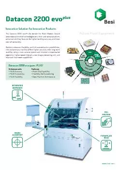
Datacon 2200 evoInnovative Solution for Innovative Products
by freya
The Datacon 2200 evo die bonder for Multi Module A...
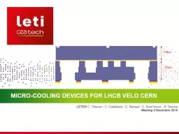
Micro-cooling devices for
by eatsui
LHCb. . Velo. CERN. . 240µm. 260µm. LETI3S ....
Introduction and application.
by giovanna-bartolotta
Ion implantation tools.. Dopant distribution.. Ma...
PiezoMEMS Foundry to Support
by luanne-stotts
PiezoMEMS Foundry to Support Research Projects N...
Integration of Electrografted
by yoshiko-marsland
Integration of Electrografted Layers for the Me...
Pre-bond TSV Test Optimization
by lois-ondreau
Pre-bond TSV Test Optimization and Stacking Yield...
SiPM Interconnections to 3D electronics
by tatyana-admore
Jelena . Ninkovic. Max-Planck-Institute for Physi...
North America Chapter MEMS/NEMS Global Technical Committee
by luanne-stotts
Micro/Nano Electromechanical Systems. Liaison Rep...
Emerging fine-pitch bump bonding techniques
by briana-ranney
Sami Vaehaenen. – CERN PH-ESE . LCD-WG4 Vertex...
Introductio n : The
by test
Genesis Allocation Committee received a request f...
The silicon substrate and adding to
by cheryl-pisano
it—Part 1. Explain . how single crystalline Si ...
Silicon Wafer Japan TC Chapter Liaison Report
by alexa-scheidler
For NA Silicon Wafer TC Chapter Meeting. In conju...
La Crosse County’s largest food pantry,
by myesha-ticknor
serving the hungry since 1986. Who comes to WAFER...
Load More...