PDF-Analog Applications Journal
26
Analog and MixedSignal Products SLYT015 May 2000
Using a decompensated op amp for
improved performance
Introduction
If your application requires
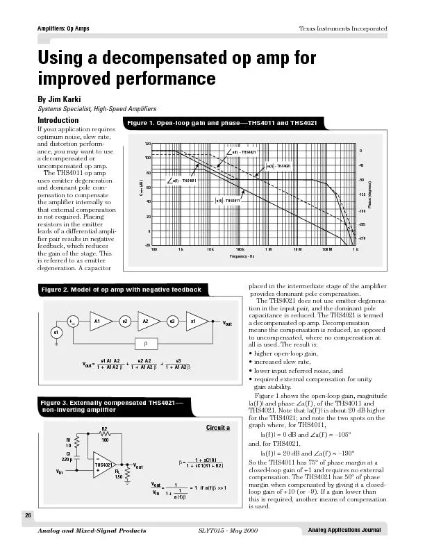
optimum noise
Download Presentation
"Analog Applications Journal" is the property of its rightful owner. Permission is granted to download and print materials on this website for personal, non-commercial use only, provided you retain all copyright notices. By downloading content from our website, you accept the terms of this agreement.
Presentation Transcript
Transcript not available.