
Computer System Architecture COMP201Th Unit: 2
Description: Computer System Architecture COMP201Th Unit: 2 Basic Computer Organization and Design Lecture: 1 Computer Registers and Bus System The organization of the computer is defined by its internal registers, the timing and control structure, and
Related Topics
Download Presentation
"Computer System Architecture COMP201Th Unit: 2" is the property of its rightful owner. Permission is granted to download and print the materials on this website for personal, non-commercial use only, and to display it on your personal computer provided you do not modify the materials and that you retain all copyright notices contained in the materials. By downloading content from our website, you accept the terms of this agreement.
Presentation Transcript
slide1. Computer System Architecture COMP201Th
Unit: 2
Basic Computer Organization and Design
Lecture: 1
Computer Registers and Bus System
The organization of the computer is defined by its internal registers, the timing and control structure, and the set of instructions that it uses. Computer can be instructed about the specific sequence of operations it must perform i.e. by means of a program.
Program: set of instructions that specify the operations, operands and sequence by which processing has to occur.
Instruction: a binary code that specifies a sequence of micro-operations for the computer.
The computer reads each instruction from memory and places it in a control register. The control then interprets the binary code of the instruction and proceeds to execute it by issuing a sequence of micro-operations.
Instruction Code: group of bits that instruct the computer to perform specific operation.
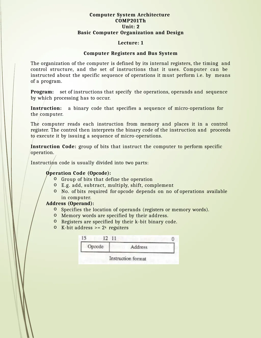
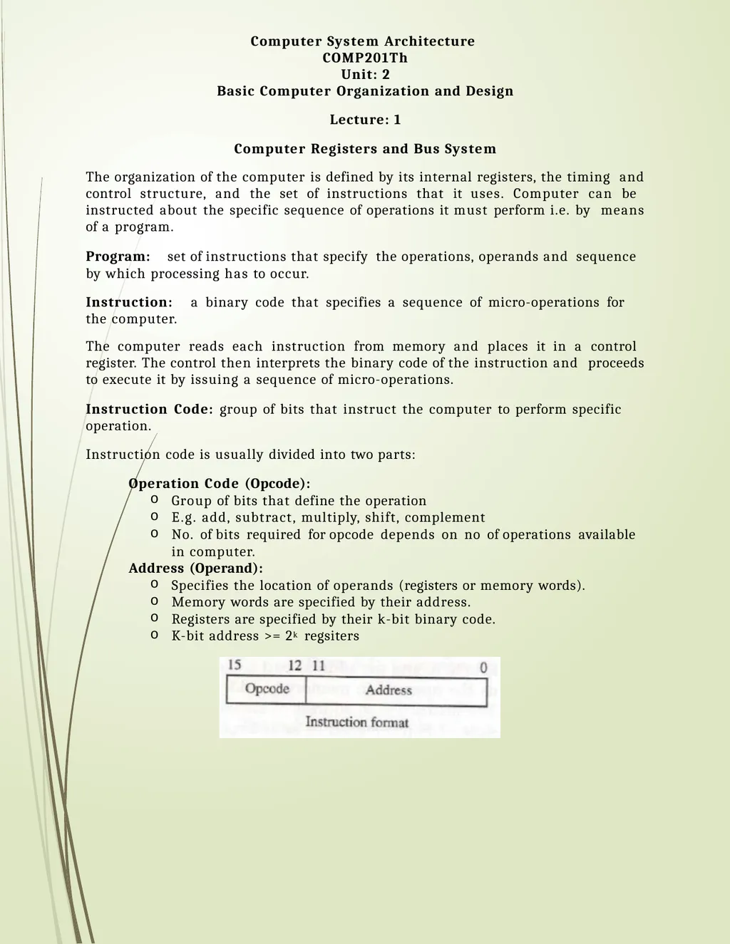
Instruction code is usually divided into two parts:
Operation Code (Opcode):
Group of bits that define the operation
E.g. add, subtract, multiply, shift, complement
No. of bits required for opcode depends on no of operations available in computer.
Address (Operand):
Specifies the location of operands (registers or memory words).
Memory words are specified by their address.
Registers are specified by their k-bit binary code.
K-bit address >= 2k regsiters<br>
slide2. Stored Program Organization:
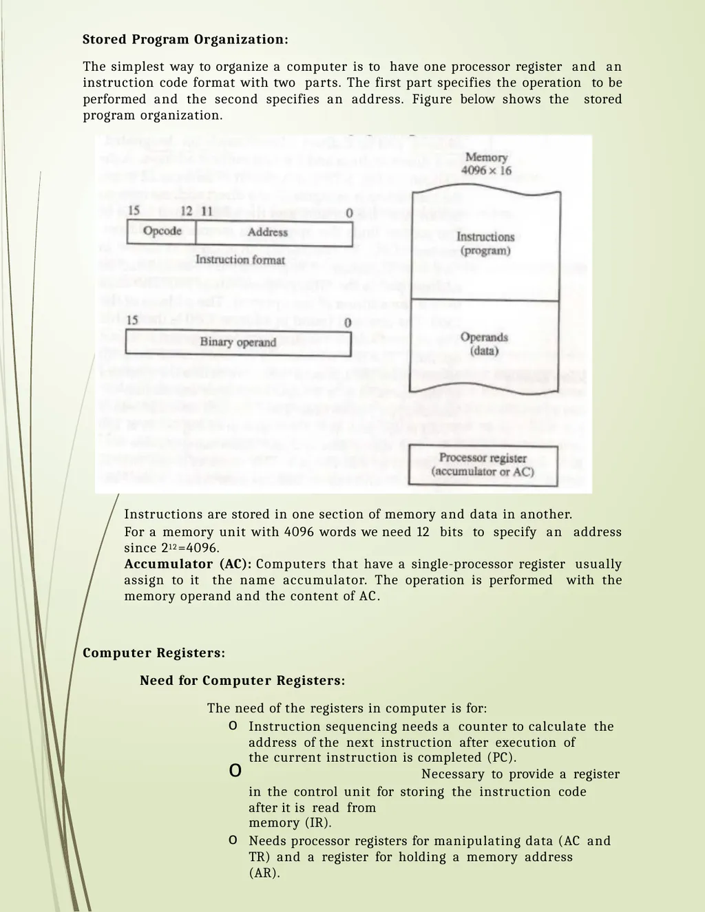
The simplest way to organize a computer is to have one processor register and an instruction code format with two parts. The first part specifies the operation to be performed and the second specifies an address. Figure below shows the stored program organization. Instructions are stored in one section of memory and data in another.
For a memory unit with 4096 words we need 12 bits to specify an address since 212=4096.
Accumulator (AC): Computers that have a single-processor register usually assign to it the name accumulator. The operation is performed with the memory operand and the content of AC.
Computer Registers:
Need for Computer Registers:
The need of the registers in computer is for:
Instruction sequencing needs a counter to calculate the address of the next instruction after execution of
the current instruction is completed (PC).
Necessary to provide a register in the control unit for storing the instruction code after it is read from
memory (IR).
Needs processor registers for manipulating data (AC and TR) and a register for holding a memory address
(AR).<br>
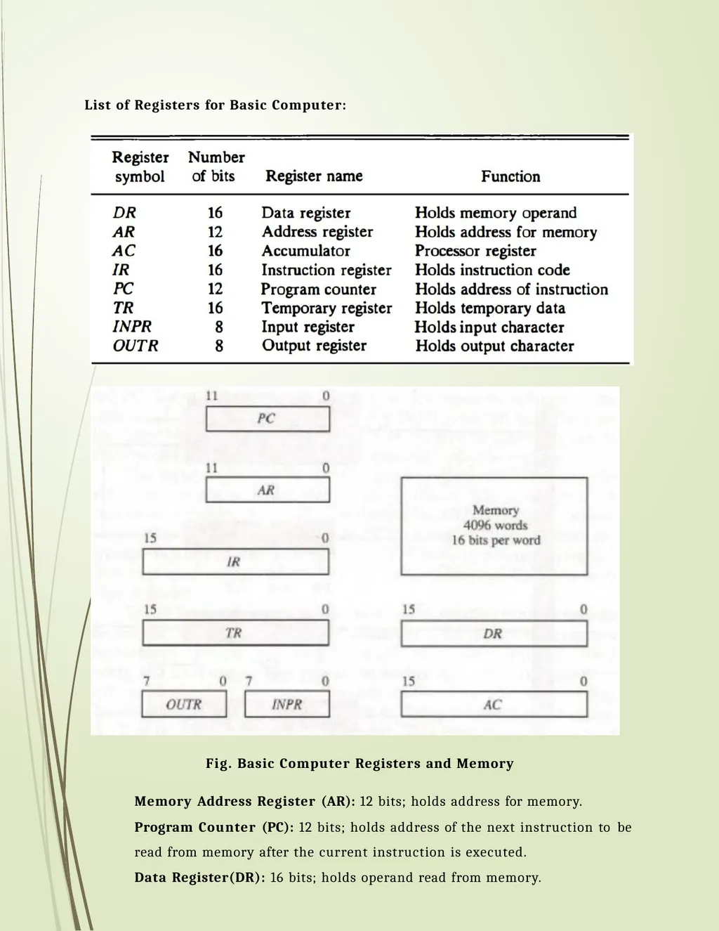
slide3. List of Registers for Basic Computer: Fig. Basic Computer Registers and Memory
Memory Address Register (AR): 12 bits; holds address for memory.
Program Counter (PC): 12 bits; holds address of the next instruction to be read from memory after the current instruction is executed.
Data Register(DR): 16 bits; holds operand read from memory.<br>
slide4. Accumulator Register (AC): 16bits; general purpose processing register.
Instruction Register (IR): 16bits; instructions read from memory are placed there.
Temporary Register (TR): 16 bits; used for holding temporary data during processing.
Input Register (INPR): 8bits; INPR receives an 8 bit character from an input device.
Output Register (OUTR): 8bits, OUTR holds an 8-bit character for an output device.<br>
slide5. Common Bus System:
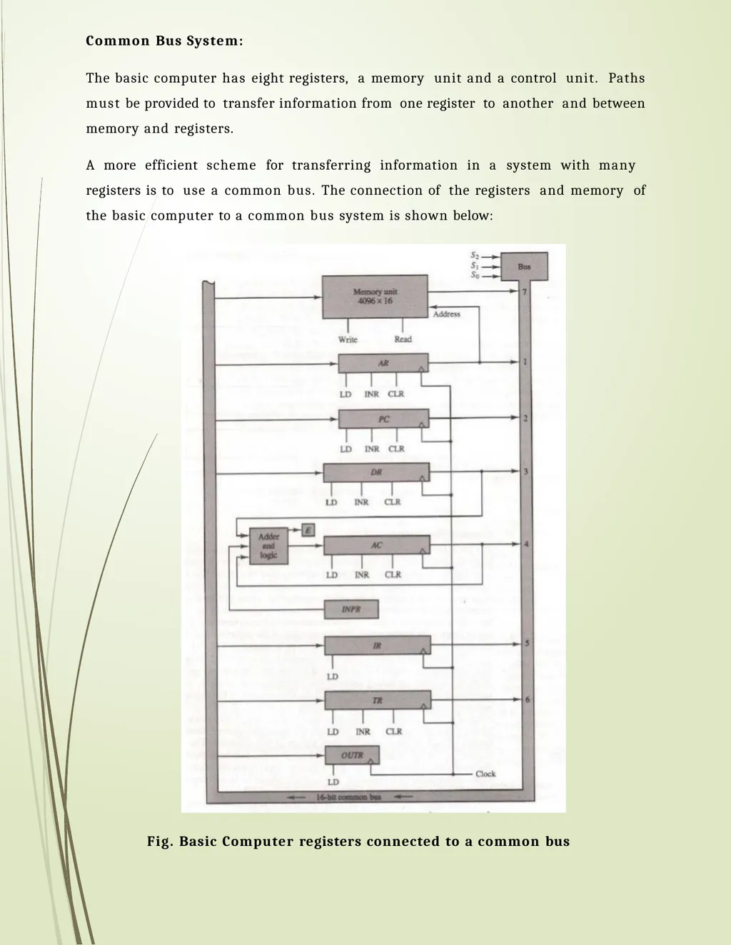
The basic computer has eight registers, a memory unit and a control unit. Paths must be provided to transfer information from one register to another and between memory and registers.
A more efficient scheme for transferring information in a system with many registers is to use a common bus. The connection of the registers and memory of the basic computer to a common bus system is shown below: Fig. Basic Computer registers connected to a common bus<br>
slide6. The outputs of seven registers and memory are connected to the common bus. The specific output that is selected for the bus lines at any given time is determined from the binary value of the selection variables S2, S1 and S0. The number along each output shows the decimal equivalents of the required binary selection.
e.g. the number along the output of DR is 3. The 16-bit outputs of DR are placed on the bus lines when S2S1S0 = 011.
The lines from the common bus are connected to the inputs of
each register and the data inputs of the memory. The particular register whose LD (Load) input is enabled receives the data from the bus during the next clock pulse transition.
The memory receives the contents of the bus when its write input is activated. The memory places its 16-bit output onto the bus when the read input is activated and S2S1S0 = 111.
Two registers AR and PC, have 12 bits each since they hold a
memory address. When the contents of AR or PC are applied to the 16-bit common bus, the four most significant bits are set to 0’s.
Five registers have three control inputs: LD (Load), INR (increment) and CLR (clear).
The input data and output data of the memory are connected to the common bus, but the memory address is connected to AR. Therefore, AR must always be used to specify a memory address.
The 16 inputs of AC come from an adder and logic circuit. This circuit has three sets of inputs:
One set of 16-bit inputs come from the outputs of AC.
Another set of 17-bit inputs come from the data register DR.
The result of an addition is transferred to AC and the end carry-out of the addition is transferred to flip-flop E (extended AC bit).
A third set of 8-bit inputs come from the input register INPR.
The content of any register can be applied onto the bus and an operation can be performed in the adder and logic circuit during the same clock cycle.<br>
Unit: 2
Basic Computer Organization and Design
Lecture: 1
Computer Registers and Bus System
The organization of the computer is defined by its internal registers, the timing and control structure, and the set of instructions that it uses. Computer can be instructed about the specific sequence of operations it must perform i.e. by means of a program.
Program: set of instructions that specify the operations, operands and sequence by which processing has to occur.
Instruction: a binary code that specifies a sequence of micro-operations for the computer.
The computer reads each instruction from memory and places it in a control register. The control then interprets the binary code of the instruction and proceeds to execute it by issuing a sequence of micro-operations.
Instruction Code: group of bits that instruct the computer to perform specific operation.
Instruction code is usually divided into two parts:
Operation Code (Opcode):
Group of bits that define the operation
E.g. add, subtract, multiply, shift, complement
No. of bits required for opcode depends on no of operations available in computer.
Address (Operand):
Specifies the location of operands (registers or memory words).
Memory words are specified by their address.
Registers are specified by their k-bit binary code.
K-bit address >= 2k regsiters<br>
slide2. Stored Program Organization:
The simplest way to organize a computer is to have one processor register and an instruction code format with two parts. The first part specifies the operation to be performed and the second specifies an address. Figure below shows the stored program organization. Instructions are stored in one section of memory and data in another.
For a memory unit with 4096 words we need 12 bits to specify an address since 212=4096.
Accumulator (AC): Computers that have a single-processor register usually assign to it the name accumulator. The operation is performed with the memory operand and the content of AC.
Computer Registers:
Need for Computer Registers:
The need of the registers in computer is for:
Instruction sequencing needs a counter to calculate the address of the next instruction after execution of
the current instruction is completed (PC).
Necessary to provide a register in the control unit for storing the instruction code after it is read from
memory (IR).
Needs processor registers for manipulating data (AC and TR) and a register for holding a memory address
(AR).<br>
slide3. List of Registers for Basic Computer: Fig. Basic Computer Registers and Memory
Memory Address Register (AR): 12 bits; holds address for memory.
Program Counter (PC): 12 bits; holds address of the next instruction to be read from memory after the current instruction is executed.
Data Register(DR): 16 bits; holds operand read from memory.<br>
slide4. Accumulator Register (AC): 16bits; general purpose processing register.
Instruction Register (IR): 16bits; instructions read from memory are placed there.
Temporary Register (TR): 16 bits; used for holding temporary data during processing.
Input Register (INPR): 8bits; INPR receives an 8 bit character from an input device.
Output Register (OUTR): 8bits, OUTR holds an 8-bit character for an output device.<br>
slide5. Common Bus System:
The basic computer has eight registers, a memory unit and a control unit. Paths must be provided to transfer information from one register to another and between memory and registers.
A more efficient scheme for transferring information in a system with many registers is to use a common bus. The connection of the registers and memory of the basic computer to a common bus system is shown below: Fig. Basic Computer registers connected to a common bus<br>
slide6. The outputs of seven registers and memory are connected to the common bus. The specific output that is selected for the bus lines at any given time is determined from the binary value of the selection variables S2, S1 and S0. The number along each output shows the decimal equivalents of the required binary selection.
e.g. the number along the output of DR is 3. The 16-bit outputs of DR are placed on the bus lines when S2S1S0 = 011.
The lines from the common bus are connected to the inputs of
each register and the data inputs of the memory. The particular register whose LD (Load) input is enabled receives the data from the bus during the next clock pulse transition.
The memory receives the contents of the bus when its write input is activated. The memory places its 16-bit output onto the bus when the read input is activated and S2S1S0 = 111.
Two registers AR and PC, have 12 bits each since they hold a
memory address. When the contents of AR or PC are applied to the 16-bit common bus, the four most significant bits are set to 0’s.
Five registers have three control inputs: LD (Load), INR (increment) and CLR (clear).
The input data and output data of the memory are connected to the common bus, but the memory address is connected to AR. Therefore, AR must always be used to specify a memory address.
The 16 inputs of AC come from an adder and logic circuit. This circuit has three sets of inputs:
One set of 16-bit inputs come from the outputs of AC.
Another set of 17-bit inputs come from the data register DR.
The result of an addition is transferred to AC and the end carry-out of the addition is transferred to flip-flop E (extended AC bit).
A third set of 8-bit inputs come from the input register INPR.
The content of any register can be applied onto the bus and an operation can be performed in the adder and logic circuit during the same clock cycle.<br>