
Focused ion beam (FIB) Overview. Ion source and
KB
Published · 31 slides · 0 views

1 / 1


Description
Focused ion beam (FIB) Overview. Ion source and optics. Ion-solid interaction, damage. Scanning ion beam imaging. ECE 730: Fabrication in the nanoscale: principles, technology and applications Instructor: Bo Cui, ECE, University of
Related Topics
Share
Embed code
Download this presentation From Below
"Focused ion beam (FIB) Overview. Ion source and" is the property of its rightful owner. Permission is granted to download and print the materials on this website for personal, non-commercial use only, and to display it on your personal computer provided you do not modify the materials and that you retain all copyright notices contained in the materials. By downloading content from our website, you accept the terms of this agreement.
Presentation Transcript
01
Focused ion beam (FIB) Overview.
Ion source and optics.
Ion-solid interaction, damage.
Scanning ion beam imaging. ECE 730: Fabrication in the nanoscale: principles, technology and applications
Instructor: Bo Cui, ECE, University of Waterloo; http://ece.uwaterloo.ca/~bcui/
Textbook: Nanofabrication: principles, capabilities and limits, by Zheng Cui<br>
Ion source and optics.
Ion-solid interaction, damage.
Scanning ion beam imaging. ECE 730: Fabrication in the nanoscale: principles, technology and applications
Instructor: Bo Cui, ECE, University of Waterloo; http://ece.uwaterloo.ca/~bcui/
Textbook: Nanofabrication: principles, capabilities and limits, by Zheng Cui<br>
02
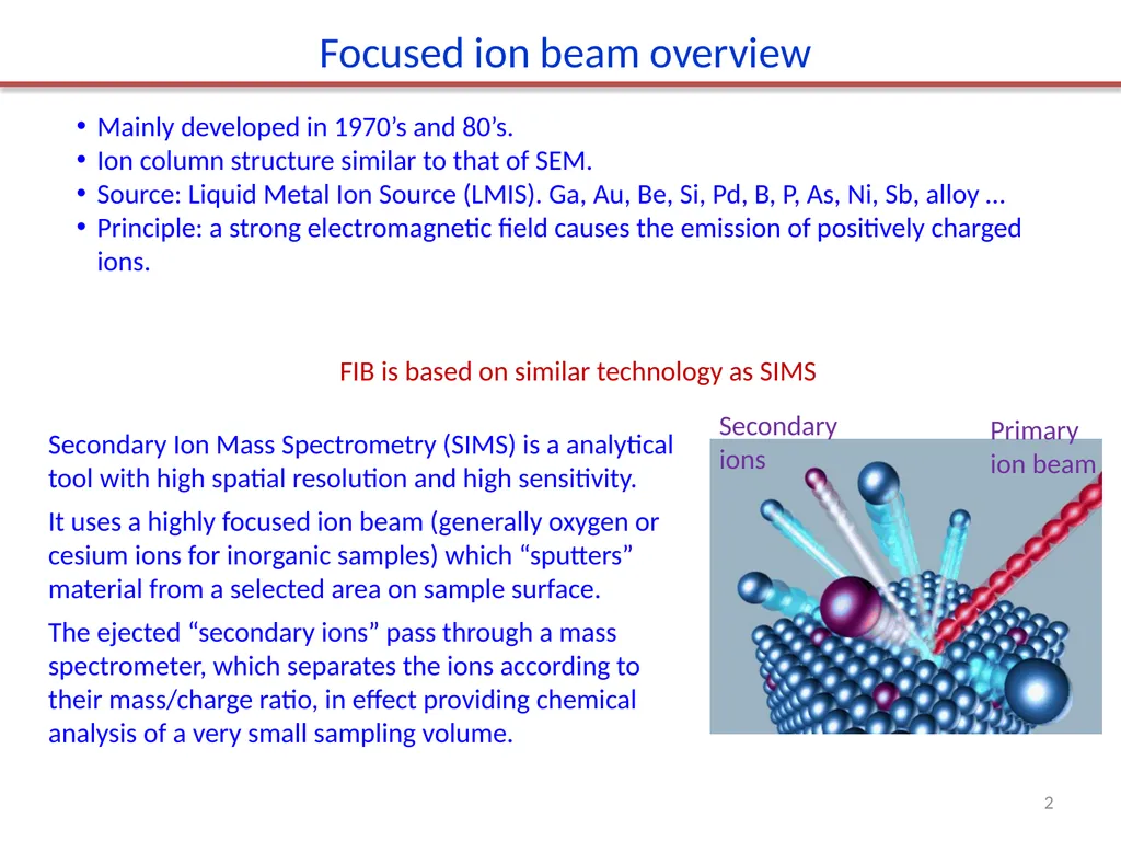
Mainly developed in 1970’s and 80’s.
Ion column structure similar to that of SEM.
Source: Liquid Metal Ion Source (LMIS). Ga, Au, Be, Si, Pd, B, P, As, Ni, Sb, alloy …
Principle: a strong electromagnetic field causes the emission of positively charged ions. Focused ion beam overview 2<br>
Ion column structure similar to that of SEM.
Source: Liquid Metal Ion Source (LMIS). Ga, Au, Be, Si, Pd, B, P, As, Ni, Sb, alloy …
Principle: a strong electromagnetic field causes the emission of positively charged ions. Focused ion beam overview 2<br>
03
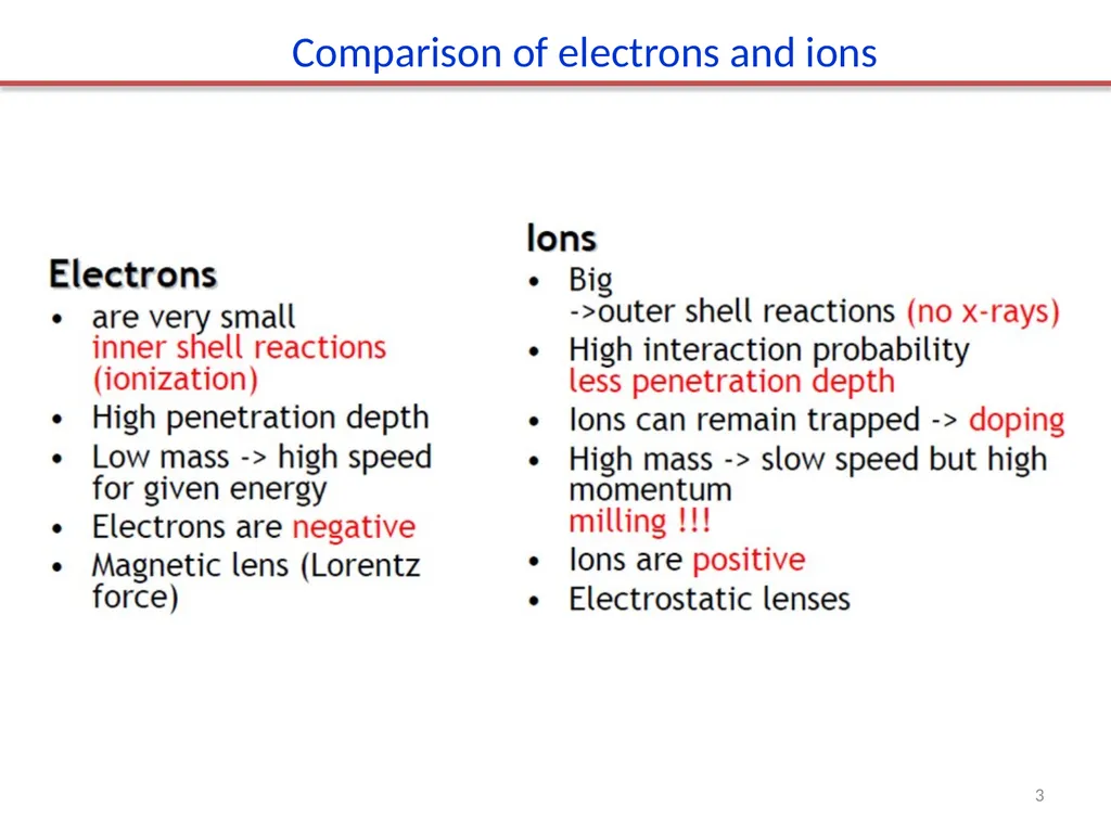
Comparison of electrons and ions 3<br>
04
Energy E=½mv2 momentum=mv=(2mE)1/2m1/2 for same E. Comparison of electrons and ions 4 For imaging<br>
05
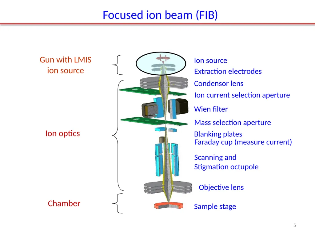
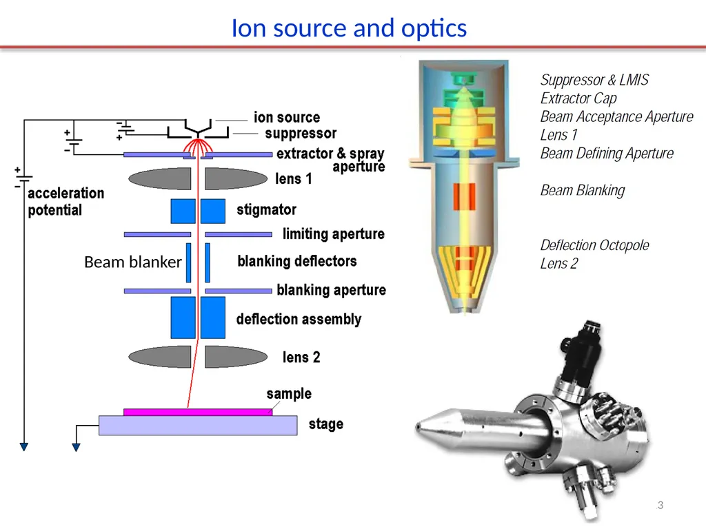
Gun with LMIS ion source Ion optics Chamber Ion source Extraction electrodes Condensor lens Ion current selection aperture Wien filter Mass selection aperture Blanking plates Faraday cup (measure current) Scanning and
Stigmation octupole Objective lens Sample stage Focused ion beam (FIB) 5<br>
Stigmation octupole Objective lens Sample stage Focused ion beam (FIB) 5<br>
06
Focused ion beam (FIB) Overview.
Ion source and optics.
Ion-solid interaction, damage.
Scanning ion beam imaging. 6<br>
Ion source and optics.
Ion-solid interaction, damage.
Scanning ion beam imaging. 6<br>
07
Ion sources Early ion sources were developed for mass spectrometry and nuclear physics research, then for ion implantation for semiconductor manufacturing.
Four types:
Electron bombardment ion sources. Gas molecules bombarded by electrons become ionized, producing a stream of ions. Small ion current and small ion energy spread, used in mass spectrometry.
Gas discharge ion source. High current, used in nuclear physics instrumentation such as high energy accelerators and ion implanters.
Field ionization source. Gas molecules absorbed on the surface of a fine needle tip can be directly ionized at extremely high electrical field near the tip apex. Used as field ion microscope to study atomic structure of a material.
Liquid metal ion source (LMIS). A field emission source from liquid metal under a strong electrical field. 7<br>
Four types:
Electron bombardment ion sources. Gas molecules bombarded by electrons become ionized, producing a stream of ions. Small ion current and small ion energy spread, used in mass spectrometry.
Gas discharge ion source. High current, used in nuclear physics instrumentation such as high energy accelerators and ion implanters.
Field ionization source. Gas molecules absorbed on the surface of a fine needle tip can be directly ionized at extremely high electrical field near the tip apex. Used as field ion microscope to study atomic structure of a material.
Liquid metal ion source (LMIS). A field emission source from liquid metal under a strong electrical field. 7<br>
08
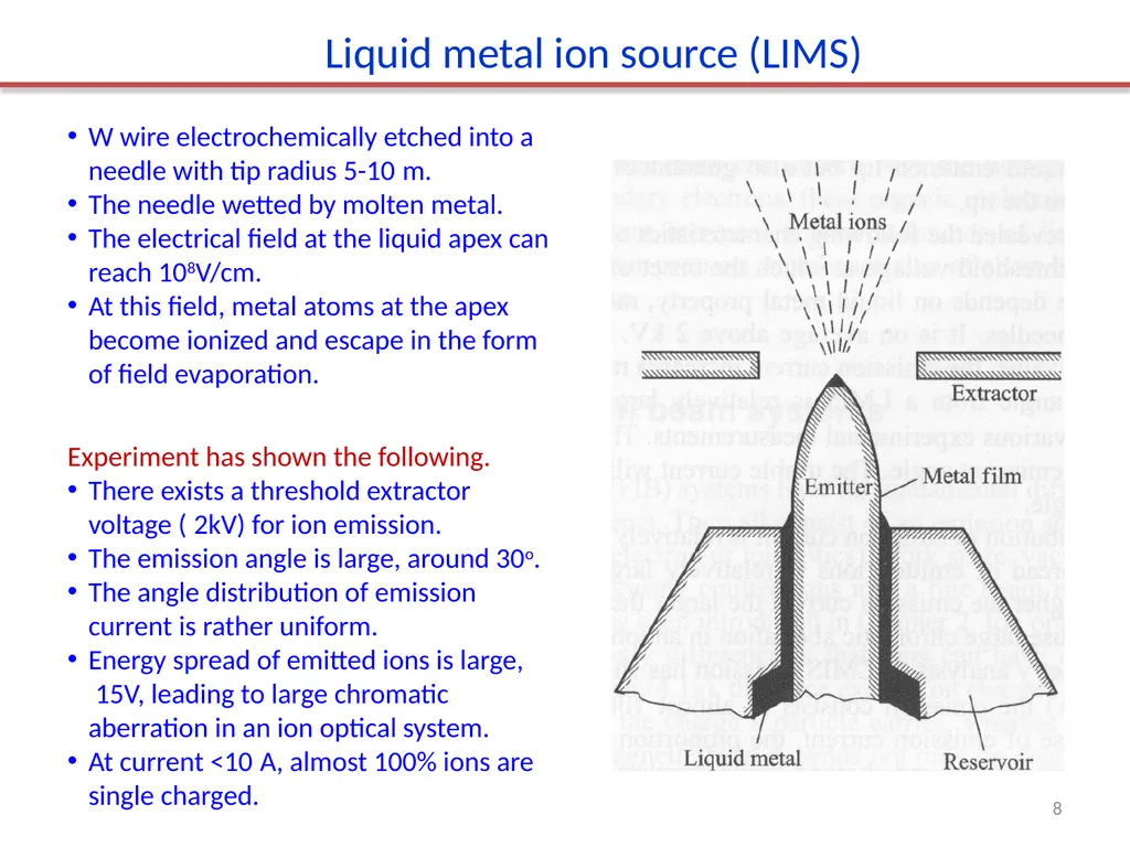
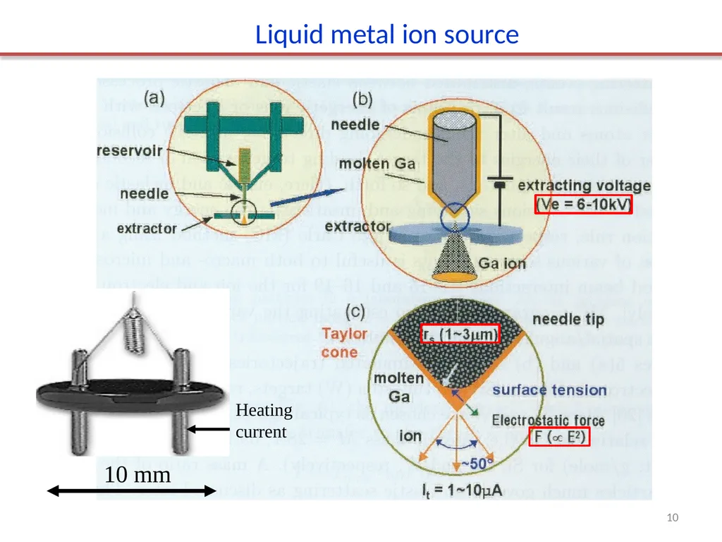
Liquid metal ion source (LIMS) W wire electrochemically etched into a needle with tip radius 5-10m.
The needle wetted by molten metal.
The electrical field at the liquid apex can reach 108V/cm.
At this field, metal atoms at the apex become ionized and escape in the form of field evaporation. Experiment has shown the following.
There exists a threshold extractor voltage (2kV) for ion emission.
The emission angle is large, around 30o.
The angle distribution of emission current is rather uniform.
Energy spread of emitted ions is large, 15V, leading to large chromatic aberration in an ion optical system.
At current <10A, almost 100% ions are single charged. 8<br>
The needle wetted by molten metal.
The electrical field at the liquid apex can reach 108V/cm.
At this field, metal atoms at the apex become ionized and escape in the form of field evaporation. Experiment has shown the following.
There exists a threshold extractor voltage (2kV) for ion emission.
The emission angle is large, around 30o.
The angle distribution of emission current is rather uniform.
Energy spread of emitted ions is large, 15V, leading to large chromatic aberration in an ion optical system.
At current <10A, almost 100% ions are single charged. 8<br>
09
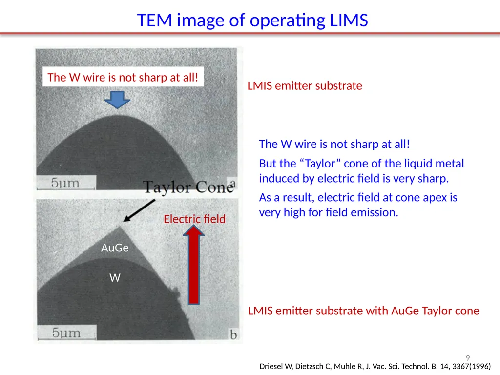
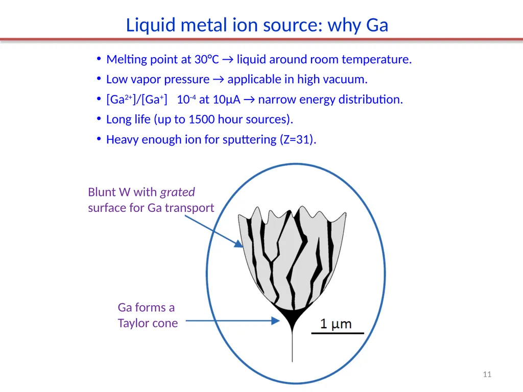
The W wire is not sharp at all!
But the “Taylor” cone of the liquid metal induced by electric field is very sharp.
As a result, electric field at cone apex is very high for field emission. TEM image of operating LIMS 9 LMIS emitter substrate LMIS emitter substrate with AuGe Taylor cone Driesel W, Dietzsch C, Muhle R, J. Vac. Sci. Technol. B, 14, 3367(1996)<br>
But the “Taylor” cone of the liquid metal induced by electric field is very sharp.
As a result, electric field at cone apex is very high for field emission. TEM image of operating LIMS 9 LMIS emitter substrate LMIS emitter substrate with AuGe Taylor cone Driesel W, Dietzsch C, Muhle R, J. Vac. Sci. Technol. B, 14, 3367(1996)<br>
10
Liquid metal ion source 10<br>
11
Liquid metal ion source: why Ga Melting point at 30°C → liquid around room temperature.
Low vapor pressure → applicable in high vacuum.
[Ga2+]/[Ga+] 10‐4 at 10μA → narrow energy distribution.
Long life (up to 1500 hour sources).
Heavy enough ion for sputtering (Z=31). 11<br>
Low vapor pressure → applicable in high vacuum.
[Ga2+]/[Ga+] 10‐4 at 10μA → narrow energy distribution.
Long life (up to 1500 hour sources).
Heavy enough ion for sputtering (Z=31). 11<br>
12
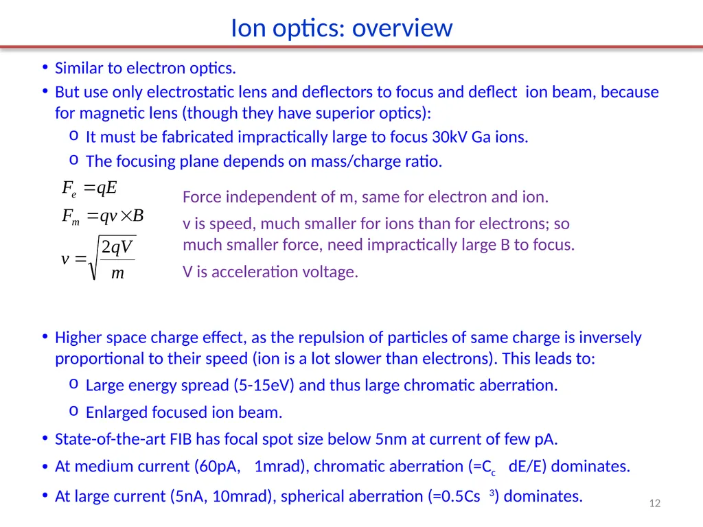
Ion optics: overview Similar to electron optics.
But use only electrostatic lens and deflectors to focus and deflect ion beam, because for magnetic lens (though they have superior optics):
It must be fabricated impractically large to focus 30kV Ga ions.
The focusing plane depends on mass/charge ratio. Force independent of m, same for electron and ion.
v is speed, much smaller for ions than for electrons; so much smaller force, need impractically large B to focus.
V is acceleration voltage. 12 Higher space charge effect, as the repulsion of particles of same charge is inversely proportional to their speed (ion is a lot slower than electrons). This leads to:
Large energy spread (5-15eV) and thus large chromatic aberration.
Enlarged focused ion beam.
State-of-the-art FIB has focal spot size below 5nm at current of few pA.
At medium current (60pA, 1mrad), chromatic aberration (=CcdE/E) dominates.
At large current (5nA, 10mrad), spherical aberration (=0.5Cs3) dominates.<br>
But use only electrostatic lens and deflectors to focus and deflect ion beam, because for magnetic lens (though they have superior optics):
It must be fabricated impractically large to focus 30kV Ga ions.
The focusing plane depends on mass/charge ratio. Force independent of m, same for electron and ion.
v is speed, much smaller for ions than for electrons; so much smaller force, need impractically large B to focus.
V is acceleration voltage. 12 Higher space charge effect, as the repulsion of particles of same charge is inversely proportional to their speed (ion is a lot slower than electrons). This leads to:
Large energy spread (5-15eV) and thus large chromatic aberration.
Enlarged focused ion beam.
State-of-the-art FIB has focal spot size below 5nm at current of few pA.
At medium current (60pA, 1mrad), chromatic aberration (=CcdE/E) dominates.
At large current (5nA, 10mrad), spherical aberration (=0.5Cs3) dominates.<br>
13
Ion source and optics 13<br>
14
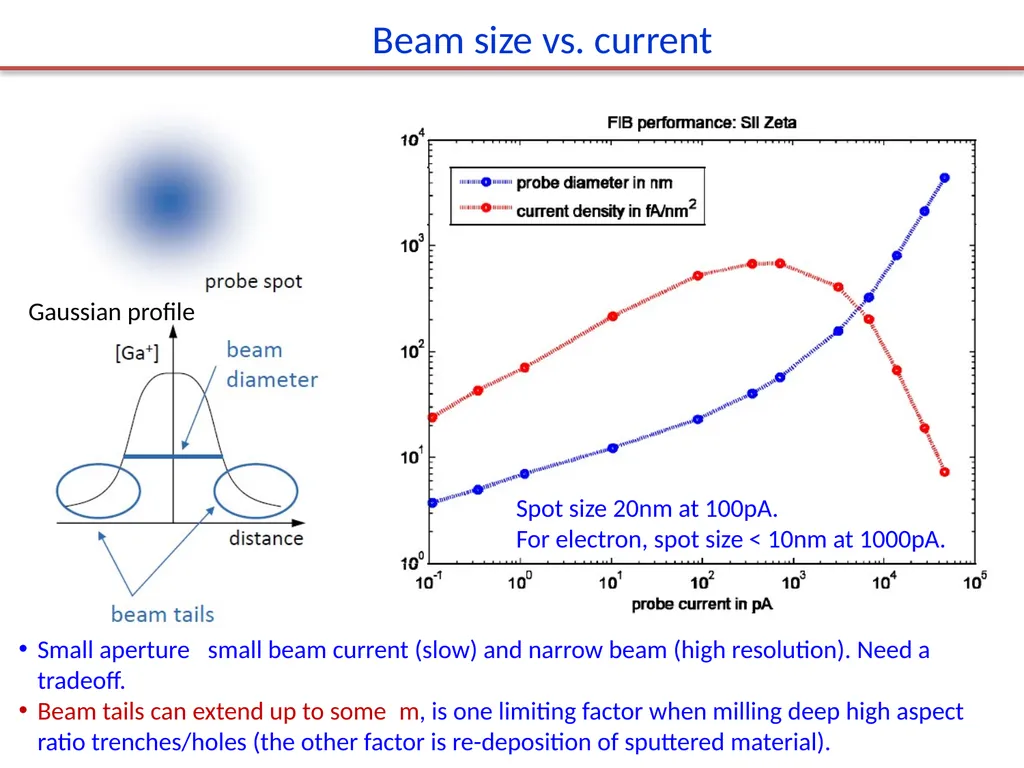
Beam size vs. current Small aperture small beam current (slow) and narrow beam (high resolution). Need a tradeoff.
Beam tails can extend up to some m, is one limiting factor when milling deep high aspect ratio trenches/holes (the other factor is re-deposition of sputtered material). 14 Spot size 20nm at 100pA.
For electron, spot size < 10nm at 1000pA. Gaussian profile<br>
Beam tails can extend up to some m, is one limiting factor when milling deep high aspect ratio trenches/holes (the other factor is re-deposition of sputtered material). 14 Spot size 20nm at 100pA.
For electron, spot size < 10nm at 1000pA. Gaussian profile<br>
15
Focused ion beam (FIB) Overview.
Ion source and optics.
Ion-solid interaction, damage.
Scanning ion beam imaging. 15<br>
Ion source and optics.
Ion-solid interaction, damage.
Scanning ion beam imaging. 15<br>
16
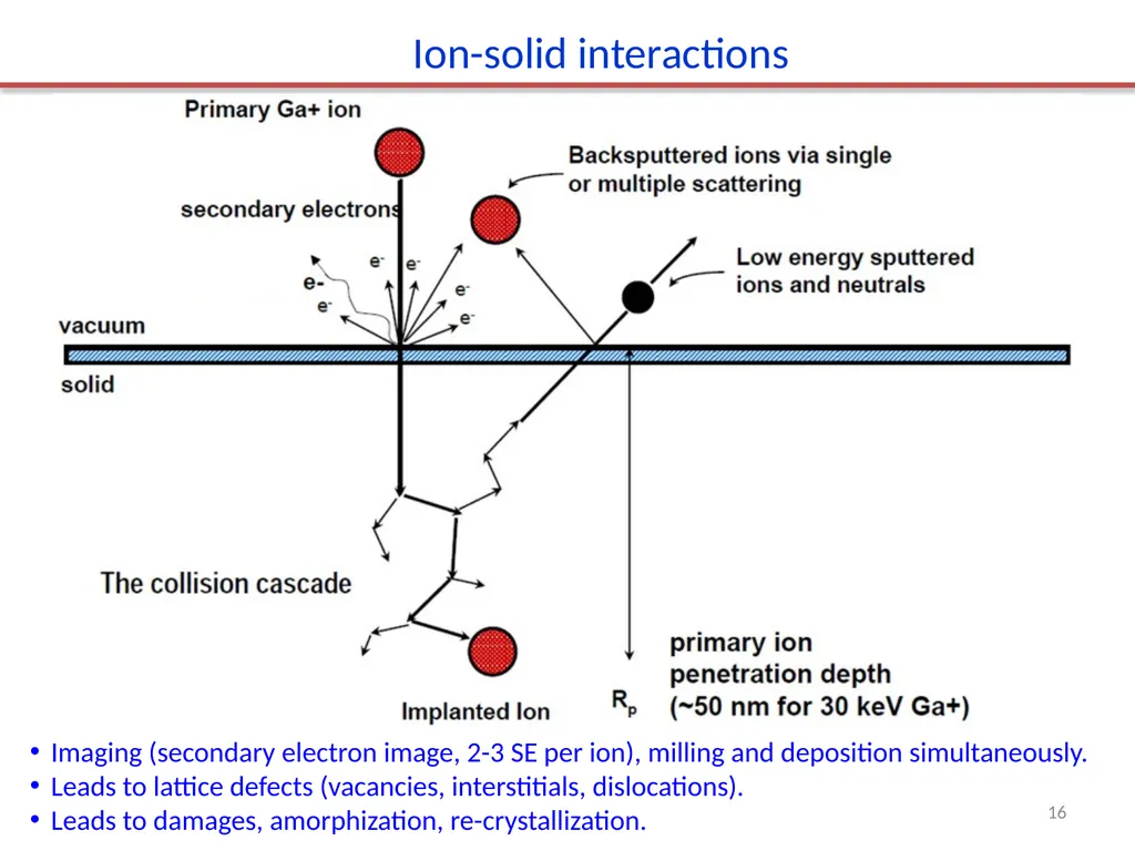
Imaging (secondary electron image, 2-3 SE per ion), milling and deposition simultaneously.
Leads to lattice defects (vacancies, interstitials, dislocations).
Leads to damages, amorphization, re-crystallization. Ion-solid interactions 16<br>
Leads to lattice defects (vacancies, interstitials, dislocations).
Leads to damages, amorphization, re-crystallization. Ion-solid interactions 16<br>
17
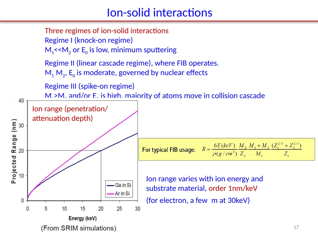
Ion-solid interactions Three regimes of ion-solid interactions
Regime I (knock-on regime)
M1<<M2 or E0 is low, minimum sputtering
Regime II (linear cascade regime), where FIB operates.
M1M2, E0 is moderate, governed by nuclear effects
Regime III (spike-on regime)
M1>M2 and/or E0 is high, majority of atoms move in collision cascade Ion range varies with ion energy and substrate material, order 1nm/keV
(for electron, a few m at 30keV) Ion range (penetration/ attenuation depth) 17<br>
Regime I (knock-on regime)
M1<<M2 or E0 is low, minimum sputtering
Regime II (linear cascade regime), where FIB operates.
M1M2, E0 is moderate, governed by nuclear effects
Regime III (spike-on regime)
M1>M2 and/or E0 is high, majority of atoms move in collision cascade Ion range varies with ion energy and substrate material, order 1nm/keV
(for electron, a few m at 30keV) Ion range (penetration/ attenuation depth) 17<br>
18
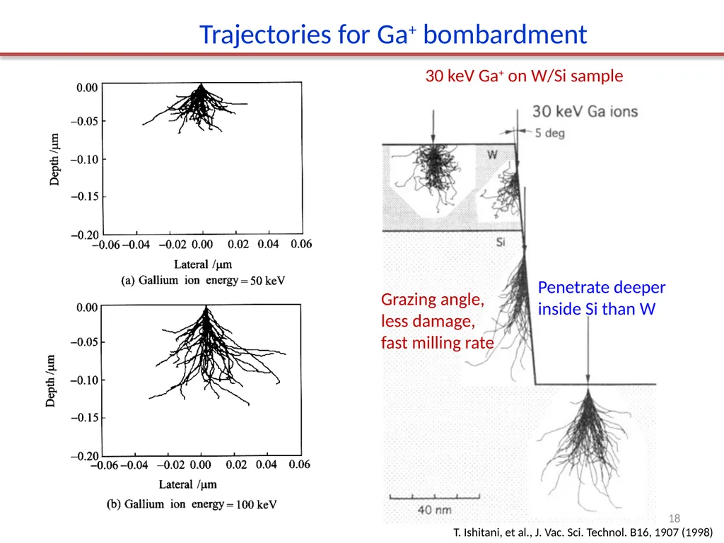
30 keV Ga+ on W/Si sample T. Ishitani, et al., J. Vac. Sci. Technol. B16, 1907 (1998) Trajectories for Ga+ bombardment Grazing angle, less damage, fast milling rate 18 Penetrate deeper inside Si than W<br>
19
Ion Implantation - Ga atoms remain in the sample target and may reach critical composition for second phase formation.
Amorphization of surface
Lattice defects
Vacancies – displaced or “missing” atoms from their equilibrium lattice positions
Interstitials – atoms which are positioned in between equilibrium lattice positions
Dislocations – a missing “half-plane” of atoms
Local heating due to large displacement of atoms that may occur within the collision cascade (10’s of nanometers from surface)
Concentration of primary defects (knock-outs from lattice sites) can be evaluated by Kinchin-Pease formula: nD = kE/2Ed, where k ≈ 0.8 is a coefficient, E is ion energy, Ed is displacement energy. Average 1000 defects per ion.
Ga in most semiconductors is acceptor, affecting electronic, optical, magnetic and thermal properties.
Concentration of Ga in the irradiated zone can be given by: CGa = 1/(1+γ), where γ is sputter yield. Damage by Ga+ bombardment 19<br>
Amorphization of surface
Lattice defects
Vacancies – displaced or “missing” atoms from their equilibrium lattice positions
Interstitials – atoms which are positioned in between equilibrium lattice positions
Dislocations – a missing “half-plane” of atoms
Local heating due to large displacement of atoms that may occur within the collision cascade (10’s of nanometers from surface)
Concentration of primary defects (knock-outs from lattice sites) can be evaluated by Kinchin-Pease formula: nD = kE/2Ed, where k ≈ 0.8 is a coefficient, E is ion energy, Ed is displacement energy. Average 1000 defects per ion.
Ga in most semiconductors is acceptor, affecting electronic, optical, magnetic and thermal properties.
Concentration of Ga in the irradiated zone can be given by: CGa = 1/(1+γ), where γ is sputter yield. Damage by Ga+ bombardment 19<br>
20
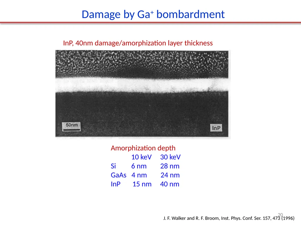
Damage by Ga+ bombardment InP, 40nm damage/amorphization layer thickness Amorphization depth
10 keV 30 keV
Si 6 nm 28 nm
GaAs 4 nm 24 nm
InP 15 nm 40 nm J. F. Walker and R. F. Broom, Inst. Phys. Conf. Ser. 157, 473 (1996) 20<br>
10 keV 30 keV
Si 6 nm 28 nm
GaAs 4 nm 24 nm
InP 15 nm 40 nm J. F. Walker and R. F. Broom, Inst. Phys. Conf. Ser. 157, 473 (1996) 20<br>
21
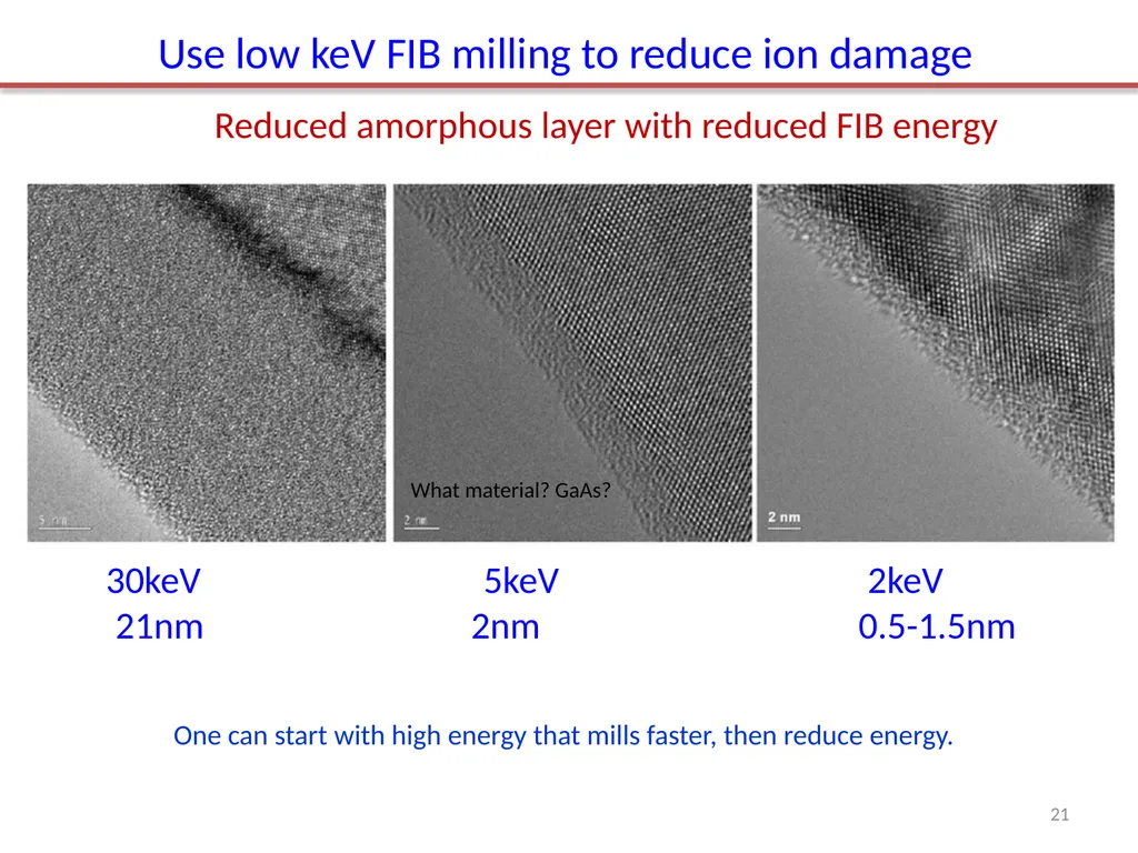
30keV 5keV 2keV
21nm 2nm 0.5-1.5nm Use low keV FIB milling to reduce ion damage Reduced amorphous layer with reduced FIB energy What material? GaAs? 21 One can start with high energy that mills faster, then reduce energy.<br>
21nm 2nm 0.5-1.5nm Use low keV FIB milling to reduce ion damage Reduced amorphous layer with reduced FIB energy What material? GaAs? 21 One can start with high energy that mills faster, then reduce energy.<br>
22
Focused ion beam (FIB) Overview.
Ion source and optics.
Ion-solid interaction, damage.
Scanning ion beam imaging. 22<br>
Ion source and optics.
Ion-solid interaction, damage.
Scanning ion beam imaging. 22<br>
23
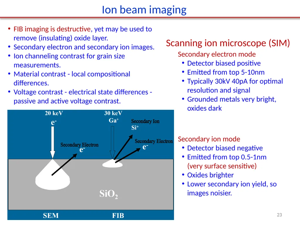
FIB imaging is destructive, yet may be used to remove (insulating) oxide layer.
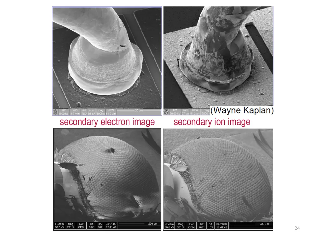
Secondary electron and secondary ion images.
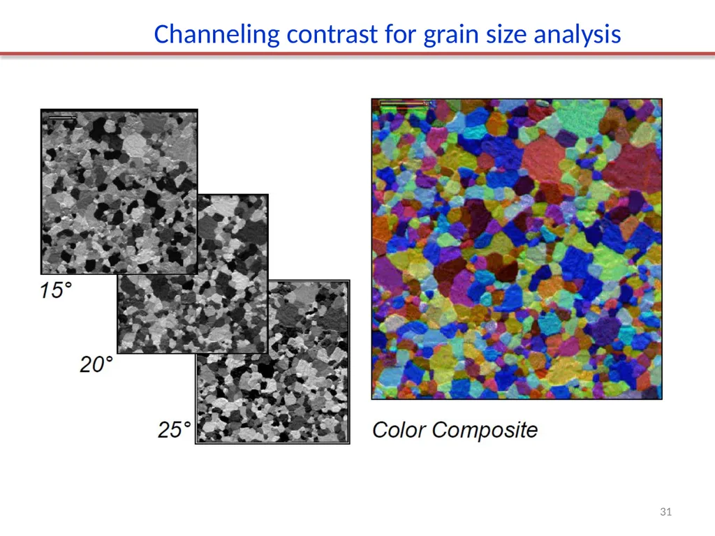
Ion channeling contrast for grain size measurements.
Material contrast - local compositional differences.
Voltage contrast - electrical state differences - passive and active voltage contrast. Ion beam imaging Secondary electron mode
Detector biased positive
Emitted from top 5-10nm
Typically 30kV 40pA for optimal resolution and signal
Grounded metals very bright, oxides dark Secondary ion mode
Detector biased negative
Emitted from top 0.5-1nm (very surface sensitive)
Oxides brighter
Lower secondary ion yield, so images noisier. 23 Scanning ion microscope (SIM)<br>
Secondary electron and secondary ion images.
Ion channeling contrast for grain size measurements.
Material contrast - local compositional differences.
Voltage contrast - electrical state differences - passive and active voltage contrast. Ion beam imaging Secondary electron mode
Detector biased positive
Emitted from top 5-10nm
Typically 30kV 40pA for optimal resolution and signal
Grounded metals very bright, oxides dark Secondary ion mode
Detector biased negative
Emitted from top 0.5-1nm (very surface sensitive)
Oxides brighter
Lower secondary ion yield, so images noisier. 23 Scanning ion microscope (SIM)<br>
24
24<br>
25
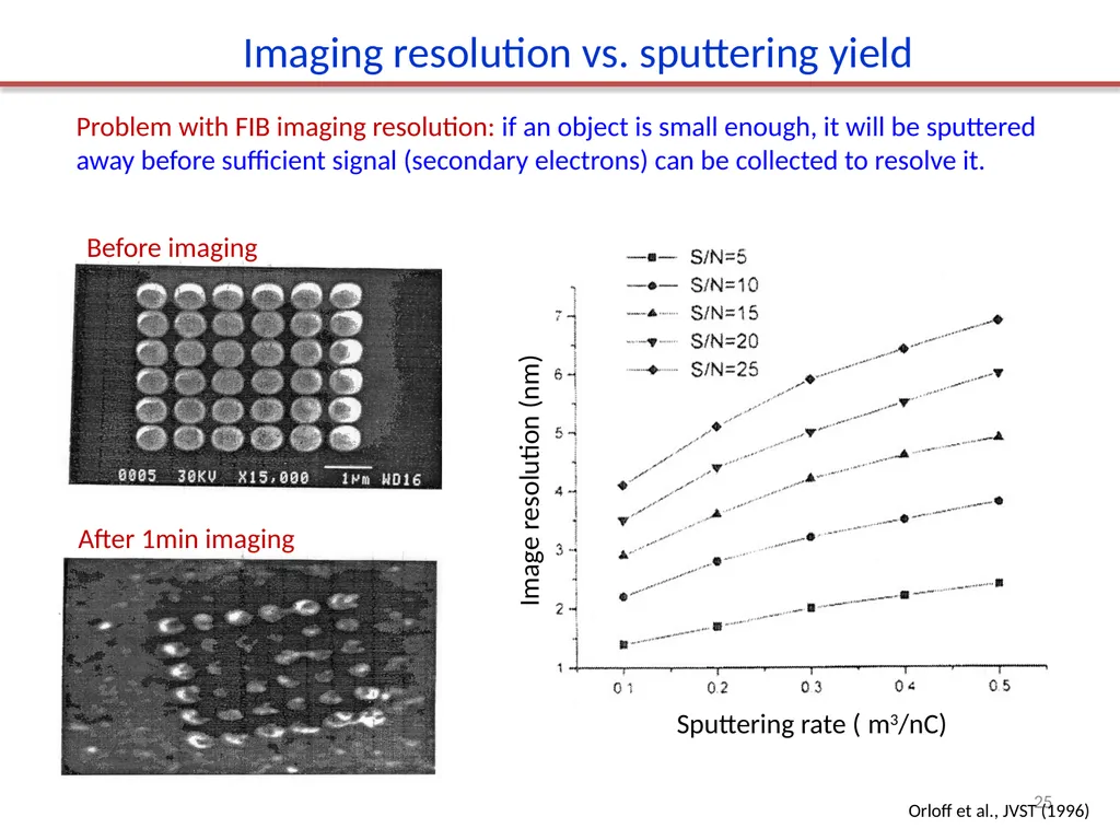
Problem with FIB imaging resolution: if an object is small enough, it will be sputtered away before sufficient signal (secondary electrons) can be collected to resolve it. Orloff et al., JVST (1996) Imaging resolution vs. sputtering yield Before imaging After 1min imaging 25<br>
26
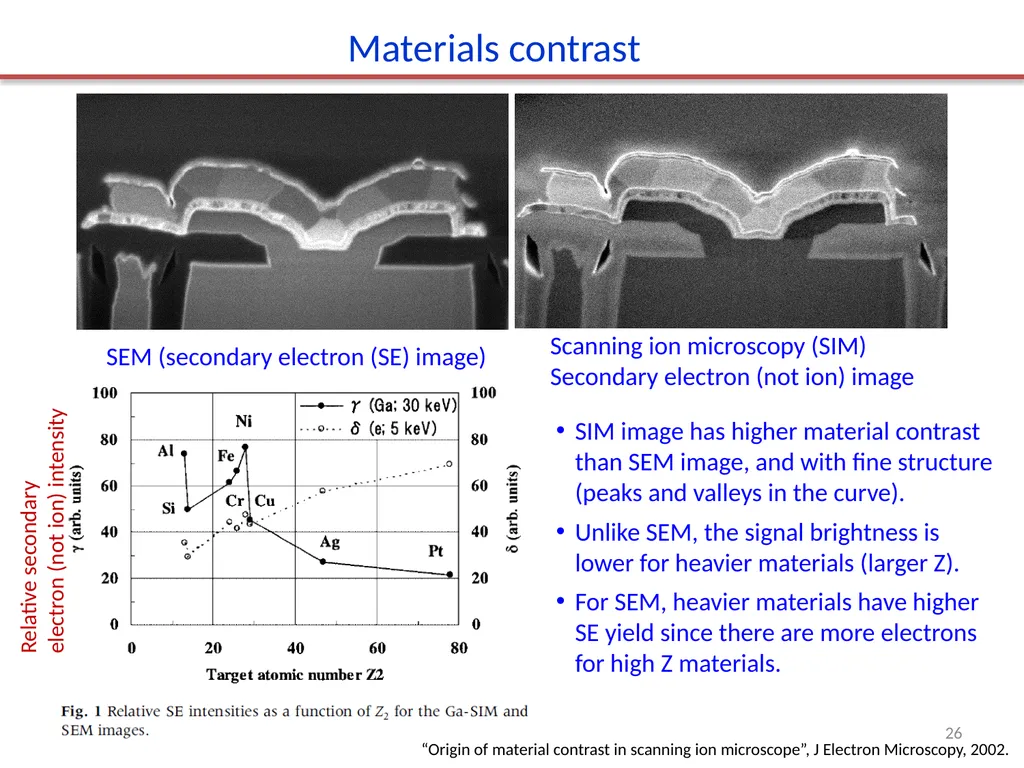
Materials contrast “Origin of material contrast in scanning ion microscope”, J Electron Microscopy, 2002. SIM image has higher material contrast than SEM image, and with fine structure (peaks and valleys in the curve).
Unlike SEM, the signal brightness is lower for heavier materials (larger Z).
For SEM, heavier materials have higher SE yield since there are more electrons for high Z materials. 26 Relative secondary electron (not ion) intensity<br>
Unlike SEM, the signal brightness is lower for heavier materials (larger Z).
For SEM, heavier materials have higher SE yield since there are more electrons for high Z materials. 26 Relative secondary electron (not ion) intensity<br>
27
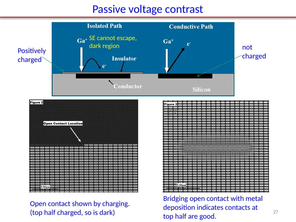
Passive voltage contrast Open contact shown by charging. (top half charged, so is dark) Bridging open contact with metal deposition indicates contacts at top half are good. SE cannot escape, dark region 27 Positively charged not charged<br>
28
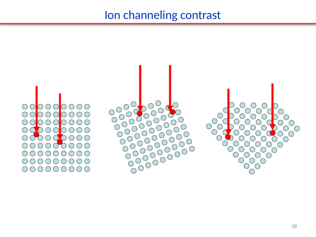
Ion channeling contrast 28<br>
29
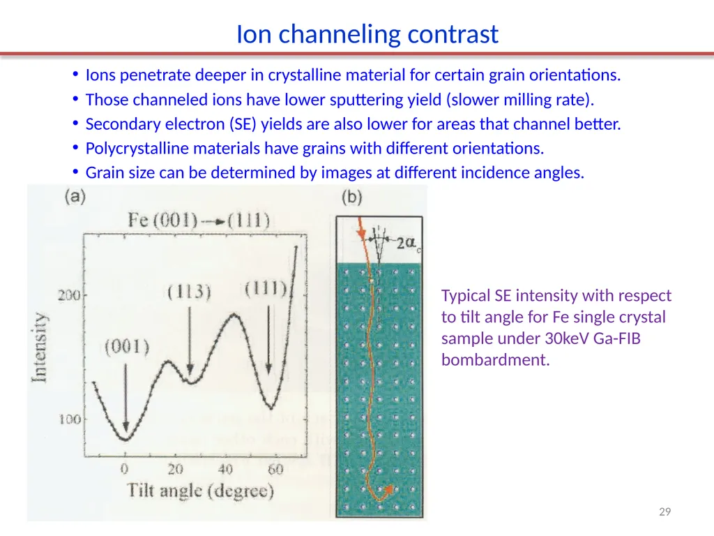
Ions penetrate deeper in crystalline material for certain grain orientations.
Those channeled ions have lower sputtering yield (slower milling rate).
Secondary electron (SE) yields are also lower for areas that channel better.
Polycrystalline materials have grains with different orientations.
Grain size can be determined by images at different incidence angles. Ion channeling contrast Typical SE intensity with respect to tilt angle for Fe single crystal sample under 30keV Ga-FIB bombardment. 29<br>
Those channeled ions have lower sputtering yield (slower milling rate).
Secondary electron (SE) yields are also lower for areas that channel better.
Polycrystalline materials have grains with different orientations.
Grain size can be determined by images at different incidence angles. Ion channeling contrast Typical SE intensity with respect to tilt angle for Fe single crystal sample under 30keV Ga-FIB bombardment. 29<br>
30
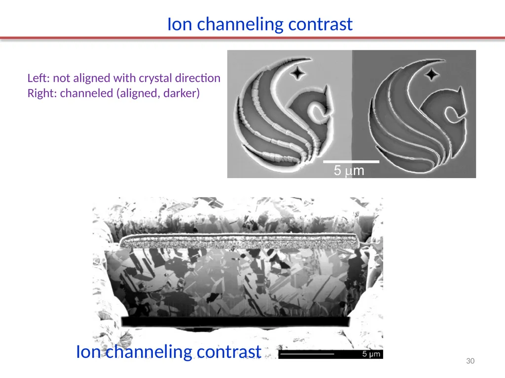
Ion channeling contrast Left: not aligned with crystal direction
Right: channeled (aligned, darker) Ion channeling contrast 30<br>
Right: channeled (aligned, darker) Ion channeling contrast 30<br>
31
Channeling contrast for grain size analysis 31<br>