Vacancy Electromigration in IC Interconnect Lines COMSOL Background As IC circuits continue to become more powerful and designed to fit into a smaller footprint, it is increasingly more important to identify and prevent any causes of
"Vacancy Electromigration in IC Interconnect Lines" is the property of its rightful owner. Permission is granted to
download and print the materials on this website for personal, non-commercial use only, and to display it
on your personal computer provided you do not modify the materials and that you retain all copyright
notices contained in the materials. By downloading content from our website, you accept the terms of this
agreement.
Presentation Transcript
01
Vacancy Electromigration in IC Interconnect Lines COMSOL<br>
02
Background As IC circuits continue to become more powerful and designed to fit into a smaller footprint, it is increasingly more important to identify and prevent any causes of failure of the circuit. One such failure mechanism is due to electromigration effects within the circuit's interconnects.
In a perfect crystal lattice, atom migration would not be possible, but all metals and metal alloys have some amount of defects. A common defect is known as a “Grain boundary” in which two different regions that have a different orientation of the crystal structure meet. Another form of a defect that occurs throughout the material is a vacancy. A vacancy is a point in the lattice where an atom should be, but is missing.
Diffusion in solids occurs due to an atom moving into a neighboring vacancy. Therefore, we can instead consider the migration of the vacancies themselves.
The migration and accumulation of vacancies within the metal is precisely what can lead to failure in an interconnect. These failures are referred to as macroscopic “voids” or “hillocks”.<br>
03
Governing Equations The overall flux of vacancies is given by: This flux considers the effects of the concentration gradient, electric field, hydrostatic stress gradient, and temperature gradient.
The vacancy balance is provided by the standard mass balance equation:<br>
04
Governing Equations cv,eq is the equilibrium vacancy concentration given by: Further, a volumetric strain is produced in the lattice by the generation of influx of a vacancy:<br>
05
Physics Interfaces Transport in Solids
Conservative form of the equation is used to solve for the transport of the vacancies.
Electric Currents
A normal current density is applied at the cathode while the anode is grounded.
Potential and electric field is computed.
Solid Mechanics
Linear Elastic Material with 2D plane strain approximation.
Inelastic Strain Rate contribution.
Domain ODE's and DAE's
It is used to solve for the total strain.<br>
06
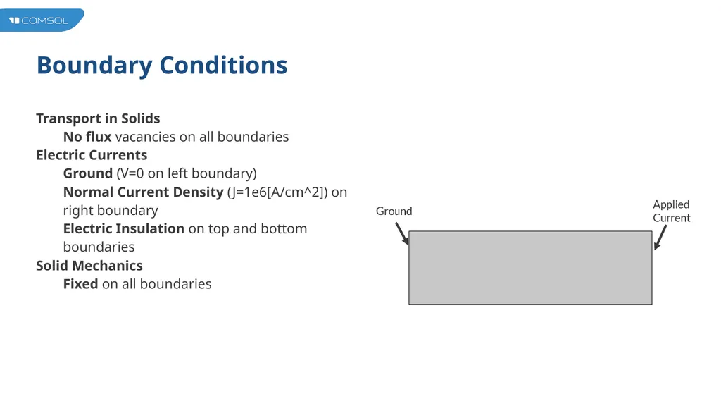
Boundary Conditions Transport in Solids
No flux vacancies on all boundaries
Electric Currents
Ground (V=0 on left boundary)
Normal Current Density (J=1e6[A/cm^2]) on right boundary
Electric Insulation on top and bottom boundaries
Solid Mechanics
Fixed on all boundaries<br>
07
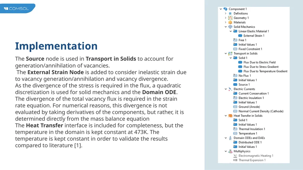
Implementation The Source node is used in Transport in Solids to account for generation/annihilation of vacancies.
The External Strain Node is added to consider inelastic strain due to vacancy generation/annihilation and vacancy divergence.
As the divergence of the stress is required in the flux, a quadratic discretization is used for solid mechanics and the Domain ODE.
The divergence of the total vacancy flux is required in the strain rate equation. For numerical reasons, this divergence is not evaluated by taking derivatives of the components, but rather, it is determined directly from the mass balance equation
The Heat Transfer interface is included for completeness, but the temperature in the domain is kept constant at 473K. The temperature is kept constant in order to validate the results compared to literature [1].<br>
08
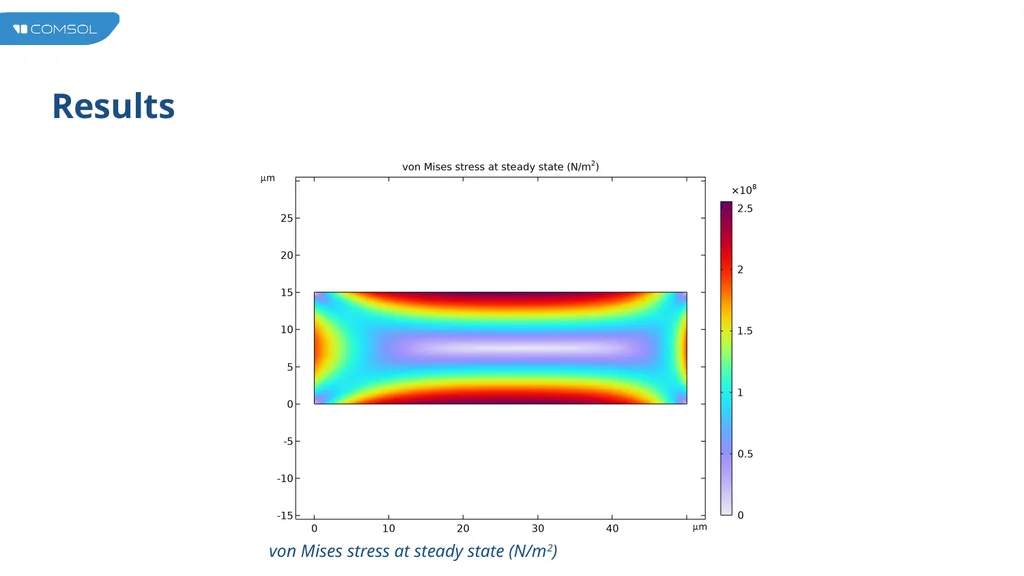
Results von Mises stress at steady state (N/m2)<br>
09
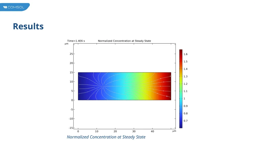
Results Normalized Concentration at Steady State<br>
10
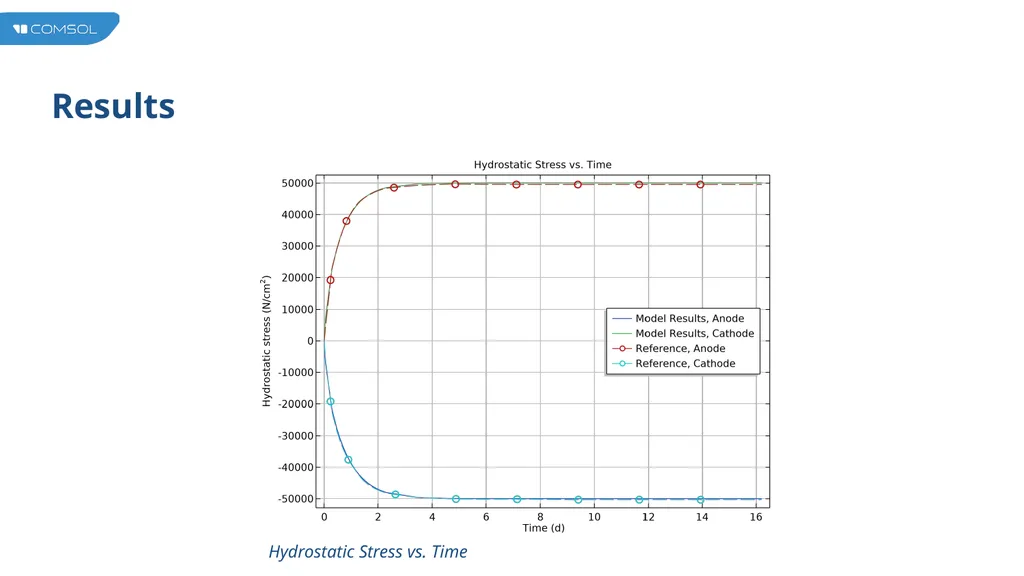
Results Hydrostatic Stress vs. Time<br>
11
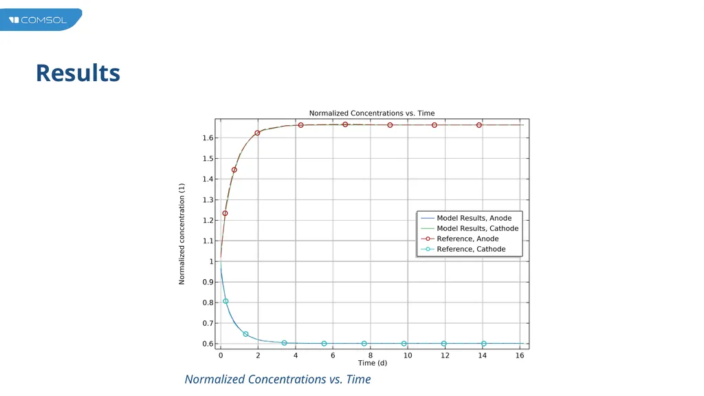
Results Normalized Concentrations vs. Time<br>
12
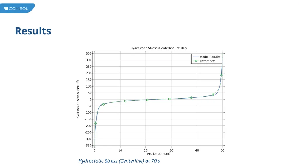
Results Hydrostatic Stress (Centerline) at 70 s<br>
13
Concluding Remarks An example of how to model the phenomenon of electromigration in IC circuit interconnects is demonstrated. This problem is inherently multiphysics in nature as it includes the transport of vacancies due to a concentration gradient, stress gradient, potential gradient, and temperature gradient. Therefore, we must solve for all of the involved physics and in a real application, also consider Joule heating and thermal expansion. The model was set up as in the reference article and the model results showed excellent agreement.<br>
14
References Hua Ye, et al. "Numerical Simulation of Stress Evolution During Electromigration in IC Interconnect Lines" IEEE Transactions on Components and Packaging Technologies, vol. 26, no. 3, Institute of Electrical and Electronics Engineers (IEEE), Sept. 2003, pp. 673-81.
Orio, R. L. de, et al. "Physically Based Models of Electromigration: From Black's Equation to Modern TCAD Models." Microelectronics Reliability, vol. 50, no. 6, Elsevier BV, June 2010, pp. 775-89.<br>