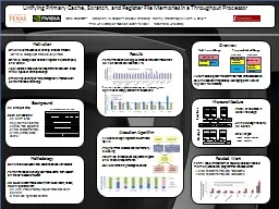
/
Unifying Primary Cache, Scratch, and Register File Memories Unifying Primary Cache, Scratch, and Register File Memories

Unifying Primary Cache, Scratch, and Register File Memories - PowerPoint Presentation

debby-jeon
debby-jeon . @debby-jeon
Follow
447 views
Uploaded On 2016-06-13

Unifying Primary Cache, Scratch, and Register File Memories - PPT Presentation

Mark Gebhart 12 Stephen W Keckler 12 Brucek Khailany 2 Ronny Krashinsky 2 William J Dally 23 1 The University of Texas at Austin 2 NVIDIA 3 Stanford University Methodology ID: 360335

shared cache register memory cache shared memory register file banks mem chip unified unit energy storage design requirements hierarchy

Share:

Link:

Embed:

Download Presentation from below link

Download Presentation The PPT/PDF document "Unifying Primary Cache, Scratch, and Reg..." is the property of its rightful owner. Permission is granted to download and print the materials on this web site for personal, non-commercial use only, and to display it on your personal computer provided you do not modify the materials and that you retain all copyright notices contained in the materials. By downloading content from our website, you accept the terms of this agreement.


Presentation Transcript

Slide1

Unifying Primary Cache, Scratch, and Register File Memories in a Throughput Processor

Mark Gebhart

1,2

Stephen W. Keckler

1,2

Brucek Khailany

2

Ronny Krashinsky

2

William J. Dally

2,31The University of Texas at Austin 2NVIDIA 3Stanford University

Methodology

Generated execution and address traces with OcelotPerformance and energy estimates come from custom SM trace-based simulator30 CUDA benchmarks drawn from CUDA SDK, Parboil, Rodinia, GPGPU-sim 22 with limited memory requirements that don’t benefit 8 that see significant benefits

Motivation

GPUs have thousands of on-chip resident threadsOn-chip storage per thread is very limitedOn-chip storage split between register file, scratchpad, and cacheApplications have diverse requirements between these three types of on-chip storageEfficiently utilizing on-chip storage can improve both performance and energy

Overview

Automated algorithm determines most efficient allocationOverheads are mitigated by leveraging prior work on register file hierarchy

Traditional Design

Proposed Unified Design

Register File

Shared Memory

Cache

Program A Program B

Register File

Shared Memory

Cache

Register File

Shared Memory

Cache

P

erformance and energy overheads for benchmarks

that do not benefit are less than 1%

Performance improvements up to 71% along with significant energy and DRAM reductions

Results

Allocation Algorithm

SIMT Lanes

SFU

TEX

MEM

ALU

Register File Hierarchy

Main Register File

Shared Memory Cache

Streaming Processor (SM)

Background

32 SMs per chip

Each SM contains:

32 SIMT lanes

Register file hierarchy

256KB main register file

64KB shared memory

64KB primary data cache

MRF

(4 banks)

MEM

Unit

Shared Memory / Cache Crossbar

Shared Memory (32 banks)

Cache (32 banks)

Cache Tags

MRF

(4 banks)

MEM

Unit

MRF

(4 banks)

MEM

Unit

Unified

(4 banks)

MEM

Unit

Shared Memory / Cache Crossbar

Cache Tags

Unified

(4 banks)

MEM

Unit

Unified

(4 banks)

MEM

Unit

Microarchitecture

Total of 96 banks

in baseline design

Unified design has only 32 banks

Challenges

:

Bank access energy

Bank conflicts

Baseline

Unified

Related Work

Allocate enough registers to eliminate spills

Programmer dictates shared memory blocking

Maximize thread count subject to register and shared requirements

Devote remaining storage to cache

Fermi

has a limited form of flexibility between shared memory

and cache, programmer chooses either:

16KB

shared memory and 48KB cache

48KB

shared memory and 16KB cache