/
Analog Applications Journal Texas Instruments Incorporated Q  www Analog Applications Journal Texas Instruments Incorporated Q  www

Analog Applications Journal Texas Instruments Incorporated Q www - PDF document

pamella-moone
pamella-moone . @pamella-moone
Follow
497 views
Uploaded On 2014-12-05

Analog Applications Journal Texas Instruments Incorporated Q www - PPT Presentation

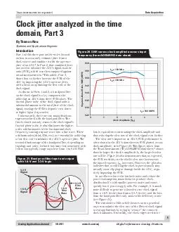
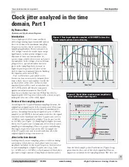
ticomaa HighPerformance Analog Products Clock jitter analyzed in the time domain Part 1 Introduction Newer highspeed ADCs come outfitted W W three to six times the maximum sampling sampling applications Recent advances in ADC design extend the usabl ID: 21252

ticomaa HighPerformance Analog Products Clock

Share:

Link:

Embed:

Download Presentation from below link

Download Pdf The PPT/PDF document "Analog Applications Journal Texas Instru..." is the property of its rightful owner. Permission is granted to download and print the materials on this web site for personal, non-commercial use only, and to display it on your personal computer provided you do not modify the materials and that you retain all copyright notices contained in the materials. By downloading content from our website, you accept the terms of this agreement.


Presentation Transcript

5 Analog Applications JournalTexas Instruments Incorporated 3Q 2010 www.ti.com/aa High-Performance Analog Products Clock jitter analyzed in the time domain, Part 1Newer high-speed ADCs come outfitted withlargbanalogSinµutbanawiath.about three to six times the maximum sampling sampling applications. Recent advances in ADC design extend the usable input range significantly so that system designers can eliminate at least one intermediate fre quency stage, which reduces cost and power consumption. In the design of an undersam pling receiver, special attention has to be Part 1 of this three-part article series focuses on how to accurately estimate jitter from a clock source and combine it with the aperture jitter of the ADC. In Part 2, that combined jitter will be used to calculate the ADC’s SNR, which will then be compared against actual measurements. Part 3 will show how to further increase the SNR of the ADC by improving the ADC’s aperture jitter, with a focus on optimizing the slew rate of the clock signal.According to the Nyquist-Shannon sampling theorem, the original input signal can be fully reconstructed if it is sampled at a rate that is at least two times its maximum fre qubncyisππumingthataninµutπignalofuµtoan63ziπ aobπn2t third, etc.] Nyquist zone is commonly referred to as under πamµlingorπubπamµlingi83owbvbrzµroµbrantiSaliaπing filtering is required in front of the ADC to sample the desired Nyquist zone and to avoid confusion when the original signal is being reconstructed.Looking closely at one sampling point reveals how timing uncbrtainty.clockjittbrorclockµhaπbnoiπb8 amplitude variation. As the input frequency increases due f1 2 Data AcquisitionBy Thomas NeuSystems and Applications Engineer –0.510203040Time Sampling Instant f= 110 MHz f= f= m7w0MHbtz uaSMaHM19 L-NNs F()L- Figure 2. Clock jitter creates more amplitude error with faster input signals Texas Instruments Incorporated 6 Analog Applications Journal High-Performance Analog Products www.ti.com/aa 3Q 2010 Data Acquisitiondetermines how fast the clock signal passes through the zero crossing point. In other words, the slew rate directly impacts the trigger threshold of the clock circuitry inside the ADC.If there is a fixed amount of thermal noise on the internal clock buffer of the ADC, then the slew rate gets converted into timing uncertainty as well, which degrades the inherent aperture jitter of the ADC. As can be seen in Figure 3, the aperture jitter is completely independent of the clock jittbr.µhaπbnoiπb8zbutthoπbtwojittbrcomµonbntπ combine at the sampling instant. Figure 3 also shows that the aperture jitter increases as the slew rate decreases. The slew rate is usually directly dependent on the clock There are several factors that limit the SNR of the ADC, πuchaπquantizationnoiπb.tyµicallynotnoticbablbin Jitter .πbb component, which is limited by the input frequency, f .abµbnaingonthbfyquiπt jittbrz , can be calculated as JitterINJitterSfR aFc ulnlog.lft8in×π×× As expected, with a fixed amount of clock jitter, the SNR degrades as the input frequency increases. This is illustrated in Figure 4, which shows the SNR of a 14-bit pipeline converter with a fixed clock jitter of 400 fs. If the input fre quency increases by one decade, such as achievable SNR due to clock jitter is reduced by 20 dB.As already mentioned, another major factor that limits the ADC’s SNR is the ADC’s thermal noise, which doesn’t change with input frequency. A 14-bit pipeline converter typically has a thermal noise of ~70 to 74 dB, also shown in Figure 4. The ADC’s thermal noise, which can be found in the data sheet, is equivalent to the SNR at the lowest specified - factori Let’s analyze the 14-bit ADC with a thermal noise of ~73 dB and a clock circuitry with 400 fs of jitter. At low input this ADC is pretty much defined by its thermal noise. As the input frequency 59m7blupL Figure 4. Fixed 400-fs clock jitter reduces SNR by 20 dB per decade increases, the 400-fs clock jitter gets more and more domi nantuntilitcomµlbtblytakbπovbrat~Gnn63ziRvbn though the SNR due to clock jitter at an input frequency thbSfRatan63zzthbtotalSfRiπabgraababyonly Thermal NoiseJitterQuantization Noise22SNRSNRSNRADCSNR dBc =20log10nnnn× (1) Texas Instruments Incorporated 7 Analog Applications Journal 3Q 2010 www.ti.com/aa High-Performance Analog Products Data Acquisition JitterSfRlnlog.lann63z3nnfπ8olaFc-n×π××- 2273dBc72dBcADCSfRlnlogantwiraFcnn-n× Now it becomes obvious that if the ADC’s thermal noise increases, the clock jitter will become very important for example, has a thermal noise floor of ~77 to 80 dB. According to the curves in Figure 4, in order to minimize the effect of clock jitter on SNR at an input frequency of 150 fs or better.As demonstrated earlier, the sample clock jitter con πiπtπofthbtiminguncbrtainty.µhaπbnoiπb8ofthb clock as well as the aperture jitter of the ADC. Those two components combine as follows: JitterJitter,Clock_InputAperture_ADCt.t8.t The aperture jitter of the ADC can be found in the data sheet. It is important to remember that this value is typically specified in combination with either clock amplitude or slew rate. Lower clock amplitudes result in slower slew rates and increase the aperture jitter accordingly. - latorzclockbuffbrzorP448iπtyµicallyπµbcifibaovbr frequency range that is offset from the fundamental onds or as a phase-noise plot, which can be integrated to obtain the jitter information. However, 10 kHz on the low bnaanaln63zonthbhighbnaarbπombtimbπnotthb right boundaries to use, as they are highly dependent upon other system parameters, as will be explained later. The importance of setting the right integration limits is illuπtratbainAigurbtzwhbrbµhaπbSnoiπbµlotiπovbrlaia with its jitter content per decade. It can be seen that the resulting jitter can be quite different if the lower limit is set to a 100-Hz or 10-kHz offset. Likewise, setting the uµµbrintbgrationlimittoanorln63zyiblaπaraπtically t2o7w109mbup LNt LNtn-. 8F()01bup Figure 5. Resulting ADC SNR is limited by thermal noise and clock jitter 1001 k10 k100 M10 M100 M 131 fs360 fs128 fs50 fs27 fs30 fs Figure 6. Jitter contribution from clock phase noise calculated per decade Texas Instruments Incorporated 8 Analog Applications Journal High-Performance Analog Products www.ti.com/aa 3Q 2010 Data AcquisitionIn the sampling process, the input signal gets mixed with the sampling clock’s signal, including its phase noise. When an FFT analysis of the input signal is performed, the primary FFT bin is centered over the input signal. The phase thbinµutπignal8abtbrminbπthbamµlituabofthbbinπ adjacent to the primary bin, as illustrated in Figure 7. Therefore, all the phase noise with an offset frequency of less than half the bin size gets lumped into the bin of the input signal and doesn’t add to the noise. Hence, the lower limit of the phase-noise integration bandwidth should be set to half the FFT bin size. The FFT bin size is calculated as follows: Sampling RateBin SizeFFT Size To further illustrate this point, an experiment using the aGaznolanaazn37zrotµointπiThbπamµlingratbwaππbt toalli776SPSzanathbclockµhaπbnoiπbiππhownin Aigurb7itS63zzwiabSbanaµaππfiltbrwaπaaabatothb clock input to limit the amount of wideband noise contributed to the jitter. A 1-GHz input signal was chosen to ensure that the SNR degradation was due solely to clock jitter. Figure 8 shows that the jitter results of the phase- - cally different for the two FFT sizes, and the SNR mea ments in Table 1 reflect that as well. Setting the proper upper integration limit Thiπiπfarmorbthanthbbntirbjittbrcontributionof~aw3fπ the chosen upper integration limit can drastically affect the calculated clock jitter and how well the predicted SNR will match the actual measurement.To determine the right limit, one has to remember something very important from the sampling process: Noise and spurs on the clock signal alias in-band from other Nyquist zones just like they would if they were if the phase noise of the clock input is not band-limited and doesn’t have a rolloff at a higher frequency, then the upper integration limit is set by the bandwidth of the itself. In some cases the clock input bandwidth can be input bandwidth of ~2 GHz to allow higher-order harmonics for very fast clock slew rates.To verify that the clock phase noise needs to be ted all the way up to the clock input bandwidth, anothbrbxµbrimbntwaππbtuµiThbs)Sr3RAtGwaπ 1 GHz to ensure that the SNR jitter was limited. Broad banawhitbnoiπbofrn63zto=3zwaπgbnbratbawith Table 1. SNR measurements for two FFT sizes FFT SIZE SNR AT 1 GHz 60 1,048,57659 51 10 Figure 7. Close-in phase noise determines amplitude of FFT bins around primary bin 101001 k10 k10 k100 M10 M100 M 500 Hz to 40 MHzt= 50 fsJitter 60 Hz to 40 MHzt= 350 fsJitter Figure 8. Integrated jitter for two FFT sizes with different lower integration limits Texas Instruments Incorporated 9 Analog Applications Journal 3Q 2010 www.ti.com/aa High-Performance Analog Products Data Acquisition an RF amplifier and added to the sampling clockaππhowninAigurbwiThbnaiffbrbnt lowSµaππfiltbrπ.4PAπ8wbrbuπbatolimit the amount of noise being added to the clock signal.The clock input bandwidth of the s)Sr3RAtGiπ~l=3zzbutπincbthbRA amplifier and the transformer both have a 3-dB bandwidth of ~1 GHz, the effective 3-dB clock input bandwidth is reduced to ~rnn63ziThbmbaπurbaSfRrbπultπin Table 2 confirm that for this setup the clock input bandwidth indeed is around rnn63zicomµariπonofthbAATµlotπin Figure 10 further confirms how the wideband noise from the RF amplifier limits the noise floor and degrades the SNR.This experiment showed that the phase noise of the clock needs to be either very low or band-limited, ideally through a tight filtbri gration limit, set by the clock bandwidth of the system, can degrade the ADC’s SNR substantially.This article has shown how to accurately estimate the sampling-clock jitter and determine the proper upper and lower integration boundaries. Part 2 will show how to use this estimation to derive the ADC’s SNR and how this result compares against actual measurements.Table 2. SNR measurements for setup in Figure 9 SETUP SNR (dBFS)No filter 39 300-MHz LPF 43 100-MHz LPF 49 1-MHz LPF 57 RFAmp Figure 9. Test setup to verify clock input noise –100304050FFTAmplitude No LPFf= 1 GHzf= 122.88 MSPSwith addednoiseINs 300-MHz LPF 100-MHz LPF 1-MHz LPF Figure 10. Overlaid measured FFT plots with different noise contributionsReference For more information related to this article, you can down load an Acrobat Reader file at www.ti.com/lit/and replace “” with the TI Lit. # for the materials listed below. Document TitleTI Lit. # 1.Thomas Neu, “Impact of sampling-clock spurs on ADC performance,” Analog Applications ....................... Related Web sitesdataconverter.ti.comwww.ti.com/sc/device/ADS54RF63 © 2010 Texas Instruments Incorporated E2E is a trademark of Texas Instruments. All other trademarks are the property of SLYT TI Worldwide Technical Support Internet Home PageTI E2E™ Community Home Page Phone+1(972) 644-5580 Brazil Phone0800-891-2616 Mexico Phone0800-670-7544 Fax+1(972) 927-6377 Internet/Email Europe, Middle East, and Africa European Free Call00800-ASK-TEXAS International+49 (0) 8161 80 2121 Russian Support+7 (4) 95 98 10 701 The European Free Call (Toll Free) number is not active in all countries. If you have technical difficulty calling the free call number, please use the international number above. Fax+(49) (0) 8161 80 2045 Internet support.ti.com/sc/pic/euro.htJapan PhoneDomestic0120-92-3326 FaxInternational+81-3-3344-5317 Domestic0120-81-0036 Internet/EmailInternational support.ti.com/sc/pic/japan.ht Domestic www.tij.co.jp/pi Asia Phone International+91-80-41381665 Domestic Toll-Free Number Taiwan Fax+886-2-2378-6808 Internet The products and services of Texas Instruments Incorporated and its subsidiaries described herein are sold subject to TI’s standard terms and conditions of sale. Customers are advised to obtain the most current and complete information about TI products and services before placing orders. TI assumes no liability for applications assistance, customer’s applications or product designs, software performance, or infringement of patents. The publication of information regarding any other company’s products or services does not constitute TI’s approval, warranty IMPORTANTNOTICETexasInstrumentsIncorporatedanditssubsidiaries(TI)reservetherighttomakecorrections,modifications,enhancements,improvements,andotherchangestoitsproductsandservicesatanytimeandtodiscontinueanyproductorservicewithoutnotice.Customersshouldobtainthelatestrelevantinformationbeforeplacingordersandshouldverifythatsuchinformationiscurrentandcomplete.AllproductsaresoldsubjecttoTI’stermsandconditionsofsalesuppliedatthetimeoforderacknowledgment.TIwarrantsperformanceofitshardwareproductstothespecificationsapplicableatthetimeofsaleinaccordancewithTI’sstandardwarranty.TestingandotherqualitycontroltechniquesareusedtotheextentTIdeemsnecessarytosupportthiswarranty.Exceptwheremandatedbygovernmentrequirements,testingofallparametersofeachproductisnotnecessarilyperformed.TIassumesnoliabilityforapplicationsassistanceorcustomerproductdesign.CustomersareresponsiblefortheirproductsandapplicationsusingTIcomponents.Tominimizetherisksassociatedwithcustomerproductsandapplications,customersshouldprovideadequatedesignandoperatingsafeguards.TIdoesnotwarrantorrepresentthatanylicense,eitherexpressorimplied,isgrantedunderanyTIpatentright,copyright,maskworkright,orotherTIintellectualpropertyrightrelatingtoanycombination,machine,orprocessinwhichTIproductsorservicesareused.InformationpublishedbyTIregardingthird-partyproductsorservicesdoesnotconstitutealicensefromTItousesuchproductsorservicesorawarrantyorendorsementthereof.Useofsuchinformationmayrequirealicensefromathirdpartyunderthepatentsorotherintellectualpropertyofthethirdparty,oralicensefromTIunderthepatentsorotherintellectualpropertyofTI.ReproductionofTIinformationinTIdatabooksordatasheetsispermissibleonlyifreproductioniswithoutalterationandisaccompaniedbyallassociatedwarranties,conditions,limitations,andnotices.Reproductionofthisinformationwithalterationisanunfairanddeceptivebusinesspractice.TIisnotresponsibleorliableforsuchaltereddocumentation.InformationofthirdpartiesmaybesubjecttoadditionalResaleofTIproductsorserviceswithstatementsdifferentfromorbeyondtheparametersstatedbyTIforthatproductorservicevoidsallexpressandanyimpliedwarrantiesfortheassociatedTIproductorserviceandisanunfairanddeceptivebusinesspractice.TIisnotresponsibleorliableforanysuchstatements.TIproductsarenotauthorizedforuseinsafety-criticalapplications(suchaslifesupport)whereafailureoftheTIproductwouldreasonablybeexpectedtocauseseverepersonalinjuryordeath,unlessofficersofthepartieshaveexecutedanagreementspecificallygoverningsuchuse.Buyersrepresentthattheyhaveallnecessaryexpertiseinthesafetyandregulatoryramificationsoftheirapplications,andacknowledgeandagreethattheyaresolelyresponsibleforalllegal,regulatoryandsafety-relatedrequirementsconcerningtheirproductsandanyuseofTIproductsinsuchsafety-criticalapplications,notwithstandinganyapplications-relatedinformationorsupportthatmaybeprovidedbyTI.Further,BuyersmustfullyindemnifyTIanditsrepresentativesagainstanydamagesarisingoutoftheuseofTIproductsinsuchsafety-criticalapplications.TIproductsareneitherdesignednorintendedforuseinmilitary/aerospaceapplicationsorenvironmentsunlesstheTIproductsarespecificallydesignatedbyTIasmilitary-gradeor"enhancedplastic."OnlyproductsdesignatedbyTIasmilitary-grademeetmilitaryspecifications.BuyersacknowledgeandagreethatanysuchuseofTIproductswhichTIhasnotdesignatedasmilitary-gradeissolelyattheBuyer'srisk,andthattheyaresolelyresponsibleforcompliancewithalllegalandregulatoryrequirementsinconnectionwithsuchuse.TIproductsareneitherdesignednorintendedforuseinautomotiveapplicationsorenvironmentsunlessthespecificTIproductsaredesignatedbyTIascompliantwithISO/TS16949requirements.Buyersacknowledgeandagreethat,iftheyuseanynon-designatedproductsinautomotiveapplications,TIwillnotberesponsibleforanyfailuretomeetsuchrequirements.FollowingareURLswhereyoucanobtaininformationonotherTexasInstrumentsproductsandapplicationsolutions: Audiowww.ti.com/audio DataConverters Automotivewww.ti.com/automotive DLP®Products Communicationsand TelecomDSPdsp.ti.com Computersand ClocksandTimers ConsumerElectronics Interfaceinterface.ti.com Energywww.ti.com/energy Logiclogic.ti.com Industrialwww.ti.com/industrial PowerMgmt Medicalwww.ti.com/medical Microcontrollersmicrocontroller.ti.com Securitywww.ti.com/security RFIDwww.ti-rfid.com Space,Avionics& RF/IFandZigBee®Solutions VideoandImaging Wirelesswww.ti.com/wireless-apps MailingAddress:TexasInstruments,PostOfficeBox655303,Dallas,Texas75265Copyright©2010,TexasInstrumentsIncorporated