/
SNALS SNALS DUAL LINE TO LINE DECODERSDEMULTIPLEXERS SDASA  APRIL   REVISED DECEMBER SNALS SNALS DUAL LINE TO LINE DECODERSDEMULTIPLEXERS SDASA  APRIL   REVISED DECEMBER

SNALS SNALS DUAL LINE TO LINE DECODERSDEMULTIPLEXERS SDASA APRIL REVISED DECEMBER - PDF document

pamella-moone
pamella-moone . @pamella-moone
Follow
537 views
Uploaded On 2014-12-13

SNALS SNALS DUAL LINE TO LINE DECODERSDEMULTIPLEXERS SDASA APRIL REVISED DECEMBER - PPT Presentation

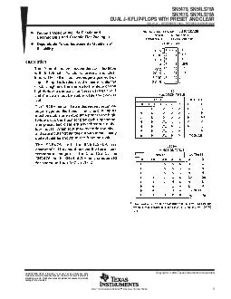
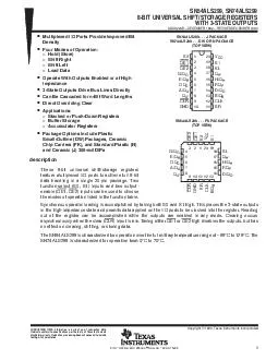
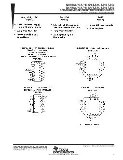
In highperformance memory systems these devices can minimize the effects of system decoding When employed with highspeed memories utilizing a fastenable circuit the delay times of these decoders and the enable time of the memory are usually less tha ID: 23598

highperformance memory systems

Share:

Link:

Embed:

Download Presentation from below link

Download Pdf The PPT/PDF document "SNALS SNALS DUAL LINE TO LINE DECODERSDE..." is the property of its rightful owner. Permission is granted to download and print the materials on this web site for personal, non-commercial use only, and to display it on your personal computer provided you do not modify the materials and that you retain all copyright notices contained in the materials. By downloading content from our website, you accept the terms of this agreement.


Presentation Transcript

DUAL 2-LINE TO 4-LINE DECODERS/DEMULTIPLEXERS SDAS204A ± APRIL 1982 ± REVISED DECEMBER 1994 1994, Texas Instruments Incorporated POST OFFICE BOX 655303 DALLAS, TEXAS 75265Memory Decoders and Data TransmissionIncorporate Two Enable Inputs to SimplifyCascading and/or Data Receptiondecoders/demultiplexers designed for use inhigh-performance memory-decoding or data-routing applications requiring very shortpropagation delay times. In high-performancememory systems, these devices can minimize theeffects of system decoding. When employed withhigh-speed memories utilizing a fast-enablecircuit, the delay times of these decoders and theenable time of the memory are usually less thanthe typical access time of the memory. Therefore,the effective system delay introduced by theSchottky-clamped system decoder is negligible.4-line decoders in a single package. Theactive-low enable (G line in demultiplexing applications. These OUTPUTS ENABLE SELECT OUTPUTS ENABLE G B A Y0 Y1 Y2 Y3 H X X H H H H L L HHH L L LHH L H L H H H H H L ...J P...D OR N P(TOP VIEW) 3212019910111213 ...FK PACKAGE(TOP VIEW) 12345678161514131291G 1A1B1Y01Y21Y3GNDV 2A2B2Y12Y2 PRODUCTION DATA information is current as of publication date.Products conform to specifications per the terms of Texas Instrumentsstandard warranty. Production processing does not necessarily includetesting of all parameters. DUAL 2-LINE TO 4-LINE DECODERS/DEMULTIPLEXERSSDAS204A ± APRIL 1982 ± REVISED DECEMBER 1994 2 POST OFFICE BOX 655303 DALLAS, TEXAS 75265logic symbols (alternatives) X/Y 121A 31B 132B EN1 15 142A 1Y040 1Y151 1Y262 1Y373 2Y012 2Y1 10 2Y39 G301G 2G DMUX 021A 131B 132B 1 15 142A 1Y040 1Y151 1Y262 1Y373 2Y012 2Y1 10 2Y39 1G 2G These symbols are in accordance with ANSI/IEEE Std 91-1984 and IEC Publication 617-12.logic diagram (positive logic) Enable 2G 1B1AEnable 1G DataOutputs 2Y3 2Y2 2Y1 2Y0 1Y3 1Y2 1Y11Y0 1231514134567 129 Pin numbers shown are for the D, J, and N packages. DUAL 2-LINE TO 4-LINE DECODERS/DEMULTIPLEXERS SDAS204A ± APRIL 1982 ± REVISED DECEMBER 1994 3 POST OFFICE BOX 655303 DALLAS, TEXAS 75265absolute maximum ratings over operating free-air temperature range (unless otherwise noted)Supply voltage, V . . . . . . . . . . . . . . . . . . . . :SN54ALS139 ±55SN74ALS139 0Storage temperature range ±65Stresses beyond those listed under ªabsolute maximum ratingsº may cause permanent damage to the device. These are stress ratings only, andfunctional operation of the device at these or any other conditions beyond those indicated under ªrecommended operating conditiimplied. Exposure to absolute-maximum-rated conditions for extended periods may affect device reliability.recommended operating conditions SN54ALS139 SN74ALS139 UNIT MIN NOM MAX MIN NOM MAX UNIT V Supply voltage 4.5 5 5.5 4.5 5 5.5 V V High-level input voltage 2 2 V V Low-level input voltage 0.7 0.8 V I ±0.4 ±0.4 mA I Low-level output current 4 8 mA TA Operating free-air temperature ±55 0 70 5C electrical characteristics over recommended operating free-air temperature range (unlessotherwise noted) PARAMETER TESTCONDITIONS SN54ALS139 SN74ALS139 UNIT PARAMETER TEST CONDITIONS MIN TYP³ MAX MIN TYP³ MAX UNIT V = 4.5 V, = ±18 mA ±1.2 ±1.2 V V = 4.5 V to 5.5 V, = ±0.4 mA ±2 ±2 V V =45V I = 4 mA 0.4 0.25 0.4 V V V = 4 . 5 V I = 8 mA 0.5 V II = 5.5 V, VI = 7 V 0.1 mA I = 5.5 V, = 2.7 V 20 20 mA I = 5.5 V, = 0.4 V ±0.1 ±0.1 mA IO§ = 5.5 V, = 2.25 V ±20 ±112 ±30 ±112 I = 5.5 V 8 13 8 13 mA = 5 V, T = 25 current, Iswitching characteristics (see Figure 1)PARAMETER FROM ( INPUT ) ( ) = 4.5 V to 5.5 V, = 50 pF, = 500 UNIT (INPUT) (OUTPUT) SN54ALS139 SN74ALS139 MIN MAX MIN MAX t AorB Y 3 3 14 ns tPHL A or B Y 3 17 3 14 ns t G Y 3 3 14 ns tPHL G Y 3 18 3 15 ns ¶For conditions shown as MIN or MAX, use the appropriate value specified under recommended operating conditions. DUAL 2-LINE TO 4-LINE DECODERS/DEMULTIPLEXERSSDAS204A ± APRIL 1982 ± REVISED DECEMBER 1994 4 POST OFFICE BOX 655303 DALLAS, TEXAS 75265PARAMETER MEASUREMENT INFORMATIONSERIES 54ALS/74ALS AND 54AS/74AS DEVICES 0.3 VFOR 3-STATE OUTPUTSUnder Test Test VOLTAGE WAVEFORMSTiming 1.3 V1.3 V VOLTAGE WAVEFORMSPULSE DURATIONS 1.3 V1.3 V1.3 V1.3 VWaveform 1Waveform 21.3 V1.3 V VOLTAGE WAVEFORMSPROPAGATION DELAY TIMESVOLTAGE WAVEFORMSENABLE AND DISABLE TIMES, 3-STATE OUTPUTS Test Under TestFOR OPEN-COLLECTOR OUTPUTS BI-STATETOTEM-POLE OUTPUTSUnder Test Test RL RL = R1 = R2 NOTES:A.C includes probe and jig capacitance.B.Waveform 1 is for an output with internal conditions such that the output is low except when disabled by the output control.Waveform 2 is for an output with internal conditions such that the output is high except when disabled by the output control.C.When measuring propagation delay items of 3-state outputs, switch S1 is open.D.All input pulses have the following characteristics: PRR E.The outputs are measured one at a time with one transition per measurement.Figure 1. Load Circuits and Voltage Waveforms PACKAGE OPTION ADDENDUM www.ti.com 28-Jul-2020 Addendum-Page 1 PACKAGING INFORMATION Orderable Device Status(1) Package Type PackageDrawing Pins PackageQty Eco Plan(2) Lead finish/Ball material(6) MSL Peak Temp(3) Op Temp (°C) Device Marking(4/5) Samples 5962-87683012A ACTIVE LCCC FK 20 1 TBD POST-PLATE N / A for Pkg Type -55 to 125 5962-87683012ASNJ54ALS139FK 5962-8768301EA ACTIVE CDIP J 16 1 TBD SNPB N / A for Pkg Type -55 to 125 5962-8768301EASNJ54ALS139J SN74ALS139D ACTIVE SOIC D 16 40 Green (RoHS& no Sb/Br) NIPDAU Level-1-260C-UNLIM 0 to 70 ALS139 SN74ALS139DR ACTIVE SOIC D 16 2500 Green (RoHS& no Sb/Br) NIPDAU Level-1-260C-UNLIM 0 to 70 ALS139 SN74ALS139N ACTIVE PDIP N 16 25 Green (RoHS& no Sb/Br) NIPDAU N / A for Pkg Type 0 to 70 SN74ALS139N SN74ALS139NE4 ACTIVE PDIP N 16 25 Green (RoHS& no Sb/Br) NIPDAU N / A for Pkg Type 0 to 70 SN74ALS139N SN74ALS139NSR ACTIVE SO NS 16 2000 Green (RoHS& no Sb/Br) NIPDAU Level-1-260C-UNLIM 0 to 70 ALS139 SNJ54ALS139FK ACTIVE LCCC FK 20 1 TBD POST-PLATE N / A for Pkg Type -55 to 125 5962-87683012ASNJ54ALS139FK SNJ54ALS139J ACTIVE CDIP J 16 1 TBD SNPB N / A for Pkg Type -55 to 125 5962-8768301EASNJ54ALS139J (1) The marketing status values are defined as follows: ACTIVE: Product device recommended for new designs. LIFEBUY: TI has announced that the device will be discontinued, and a lifetime-buy period is in effect. NRND: Not recommended for new designs. Device is in production to support existing customers, but TI does not recommend using this part in a new design. PREVIEW: Device has been announced but is not in production. Samples may or may not be available. OBSOLETE: TI has discontinued the production of the device. (2) RoHS: TI defines "RoHS" to mean semiconductor products that are compliant with the current EU RoHS requirements for all 10 RoHS substances, including the requirement that RoHS substancedo not exceed 0.1% by weight in homogeneous materials. Where designed to be soldered at high temperatures, "RoHS" products are suitable for use in specified lead-free processes. TI mayreference these types of products as "Pb-Free". RoHS Exempt: TI defines "RoHS Exempt" to mean products that contain lead but are compliant with EU RoHS pursuant to a specific EU RoHS exemption. Green: TI defines "Green" to mean the content of Chlorine (Cl) and Bromine (Br) based flame retardants meet JS709B low halogen requirements of threshold. Antimony trioxide basedflame retardants must also meet the threshold requirement. PACKAGE OPTION ADDENDUM www.ti.com 28-Jul-2020 Addendum-Page 2 (3) MSL, Peak Temp. - The Moisture Sensitivity Level rating according to the JEDEC industry standard classifications, and peak solder temperature. (4) There may be additional marking, which relates to the logo, the lot trace code information, or the environmental category on the device. (5) Multiple Device Markings will be inside parentheses. Only one Device Marking contained in parentheses and separated by a "~" will appear on a device. If a line is indented then it is a continuationof the previous line and the two combined represent the entire Device Marking for that device. (6) Lead finish/Ball material - Orderable Devices may have multiple material finish options. Finish options are separated by a vertical ruled line. Lead finish/Ball material values may wrap to twolines if the finish value exceeds the maximum column width. Important Information and Disclaimer:The information provided on this page represents TI's knowledge and belief as of the date that it is provided. TI bases its knowledge and belief on informationprovided by third parties, and makes no representation or warranty as to the accuracy of such information. Efforts are underway to better integrate information from third parties. TI has taken andcontinues to take reasonable steps to provide representative and accurate information but may not have conducted destructive testing or chemical analysis on incoming materials and chemicals.TI and TI suppliers consider certain information to be proprietary, and thus CAS numbers and other limited information may not be available for release. In no event shall TI's liability arising out of such information exceed the total purchase price of the TI part(s) at issue in this document sold by TI to Customer on an annual basis. OTHER QUALIFIED VERSIONS OF SN54ALS139, SN74ALS139 :•Catalog: SN74ALS139•Military: SN54ALS139 NOTE: Qualified Version Definitions:•Catalog - TI's standard catalog product•Military - QML certified for Military and Defense Applications TAPEANDREELINFORMATION *Alldimensionsarenominal Device PackageType PackageDrawing Pins SPQ ReelDiameter(mm) ReelWidthW1(mm) A0(mm) B0(mm) K0(mm) P1(mm) W(mm) Pin1Quadrant SN74ALS139DR SOIC D 16 2500 330.0 16.4 6.5 10.3 2.1 8.0 16.0 Q1 SN74ALS139NSR SO NS 16 2000 330.0 16.4 8.2 10.5 2.5 12.0 16.0 Q1 PACKAGEMATERIALSINFORMATIONwww.ti.com14-Jul-2012 PackMaterials-Page1 *Alldimensionsarenominal Device PackageType PackageDrawing Pins SPQ Length(mm) Width(mm) Height(mm) SN74ALS139DR SOIC D 16 2500 333.2 345.9 28.6 SN74ALS139NSR SO NS 16 2000 367.0 367.0 38.0 PACKAGEMATERIALSINFORMATIONwww.ti.com14-Jul-2012 PackMaterials-Page2 IMPORTANTNOTICEANDDISCLAIMER “ASIS”