
Instructor: Alan L. Cox The Memory Hierarchy COMP
JO
Published · 88 slides · 0 views
1 / 1
Description
Instructor: Alan L. Cox The Memory Hierarchy COMP 222: Introduction to Computer Organization Many slides adapted from Bryant and OHallaron, Computer Systems: A Programmers Perspective, Third Edition The Memory Hierarchy The memory
Related Topics
Share
Embed code
Download this presentation From Below
"Instructor: Alan L. Cox The Memory Hierarchy COMP" is the property of its rightful owner. Permission is granted to download and print the materials on this website for personal, non-commercial use only, and to display it on your personal computer provided you do not modify the materials and that you retain all copyright notices contained in the materials. By downloading content from our website, you accept the terms of this agreement.
Presentation Transcript
01
Instructor:
Alan L. Cox The Memory Hierarchy COMP 222: Introduction to Computer Organization Many slides adapted from Bryant and O’Hallaron, Computer Systems: A Programmer’s Perspective, Third Edition<br>
Alan L. Cox The Memory Hierarchy COMP 222: Introduction to Computer Organization Many slides adapted from Bryant and O’Hallaron, Computer Systems: A Programmer’s Perspective, Third Edition<br>
02
The Memory Hierarchy The memory abstraction
Random-Access Memory (RAM): main memory building block
Locality of reference
The memory hierarchy
Storage technologies and trends<br>
Random-Access Memory (RAM): main memory building block
Locality of reference
The memory hierarchy
Storage technologies and trends<br>
03
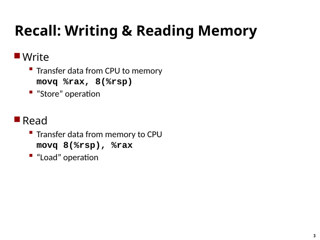
Recall: Writing & Reading Memory Write
Transfer data from CPU to memory movq %rax, 8(%rsp)
“Store” operation
Read
Transfer data from memory to CPU movq 8(%rsp), %rax
“Load” operation<br>
Transfer data from CPU to memory movq %rax, 8(%rsp)
“Store” operation
Read
Transfer data from memory to CPU movq 8(%rsp), %rax
“Load” operation<br>
04
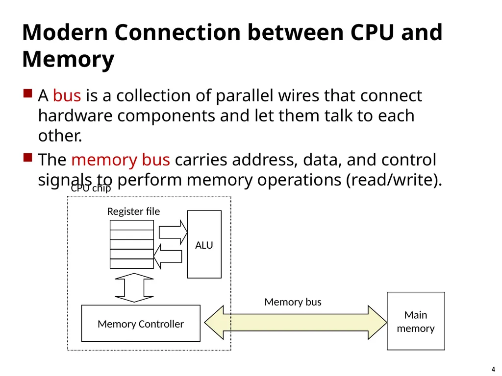
Modern Connection between CPU and Memory A bus is a collection of parallel wires that connect hardware components and let them talk to each other.
The memory bus carries address, data, and control signals to perform memory operations (read/write). Register file CPU chip Memory bus<br>
The memory bus carries address, data, and control signals to perform memory operations (read/write). Register file CPU chip Memory bus<br>
05
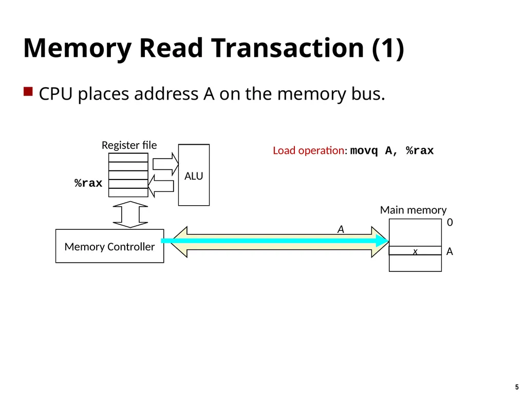
Memory Read Transaction (1) CPU places address A on the memory bus. Register file 0 A Main memory %rax Load operation: movq A, %rax<br>
06
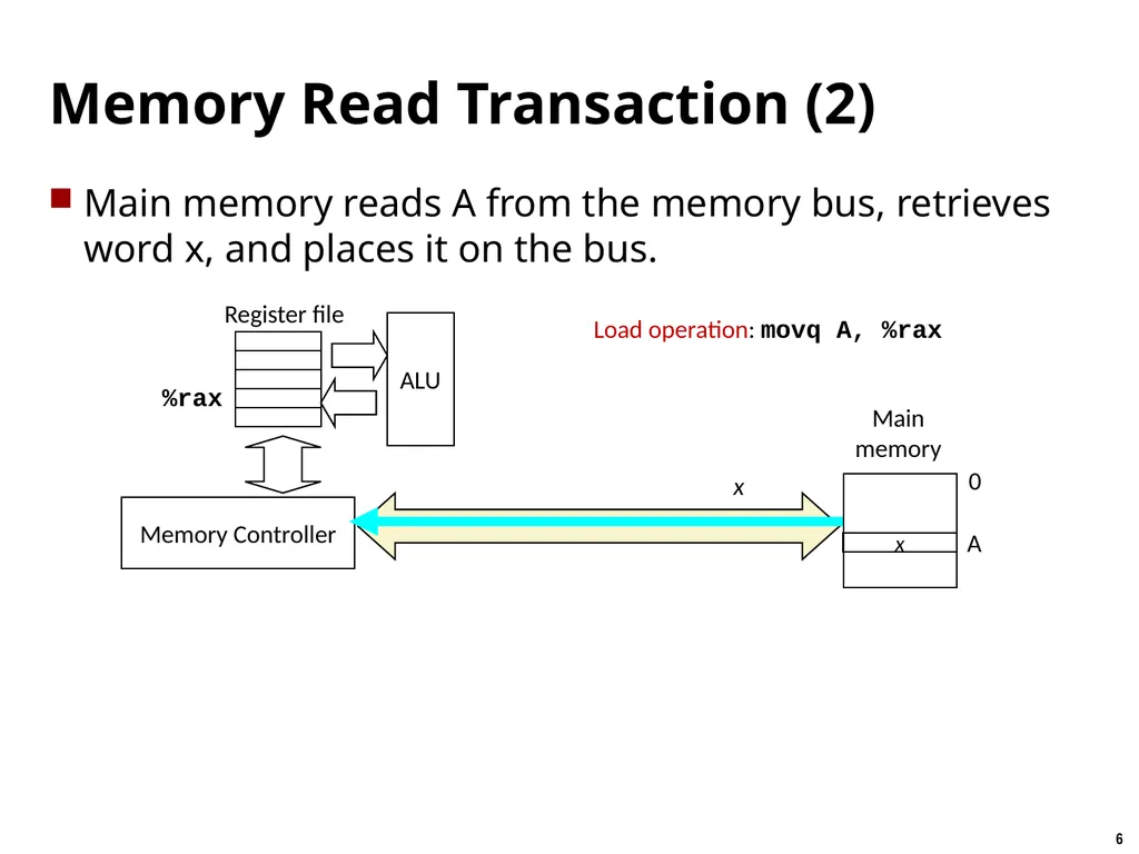
Memory Read Transaction (2) Main memory reads A from the memory bus, retrieves word x, and places it on the bus. Register file 0 A Main memory %rax Load operation: movq A, %rax<br>
07
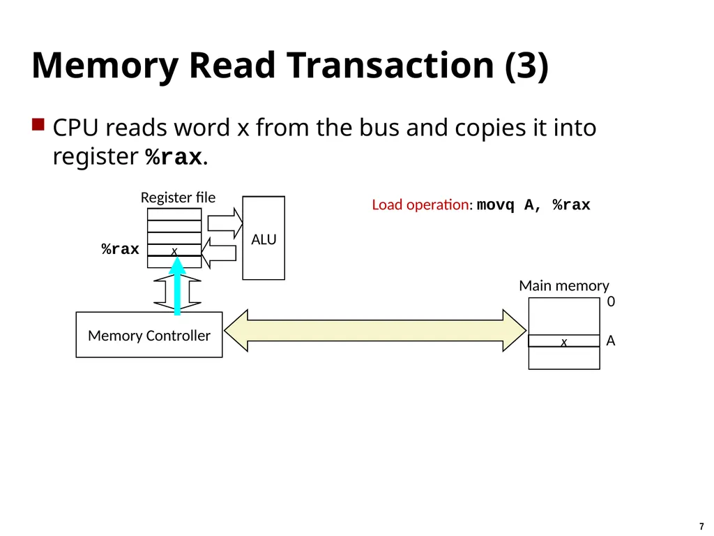
Memory Read Transaction (3) CPU reads word x from the bus and copies it into register %rax. Register file Main memory 0 A %rax Load operation: movq A, %rax<br>
08
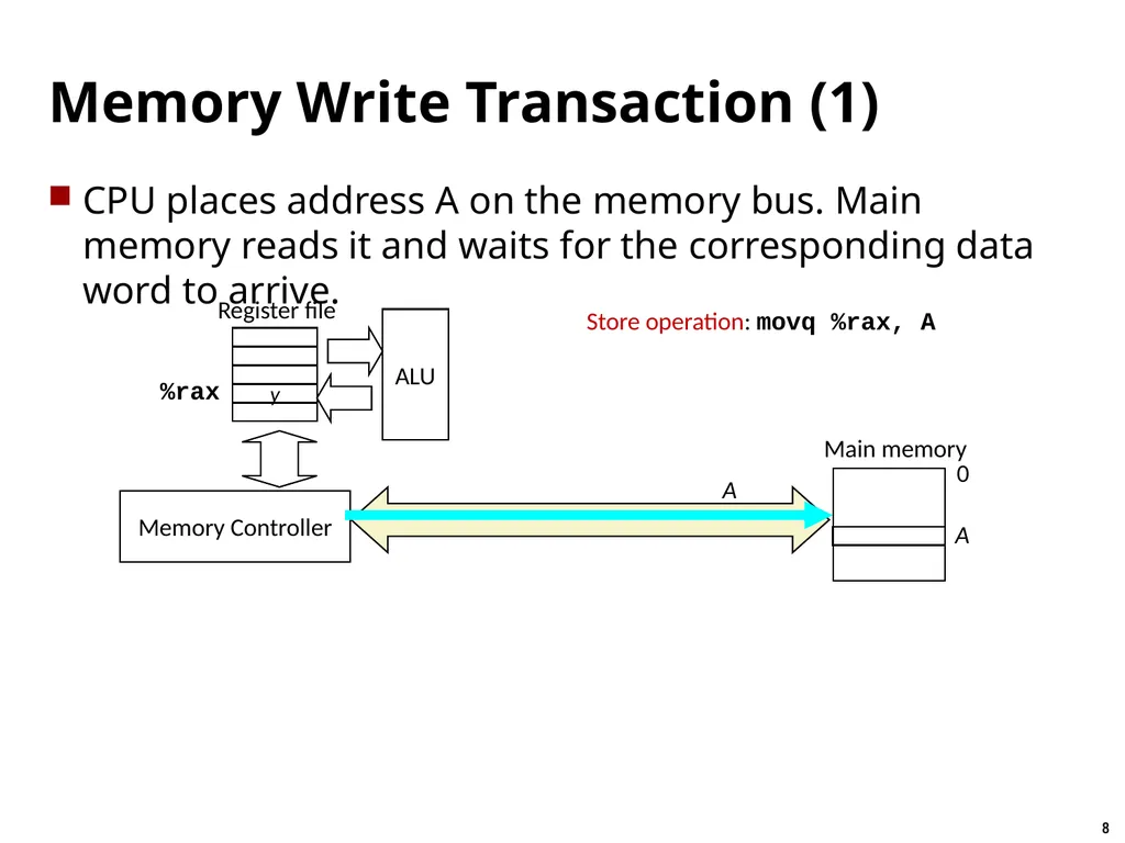
Memory Write Transaction (1) CPU places address A on the memory bus. Main memory reads it and waits for the corresponding data word to arrive. Register file Main memory 0 A %rax Store operation: movq %rax, A<br>
09
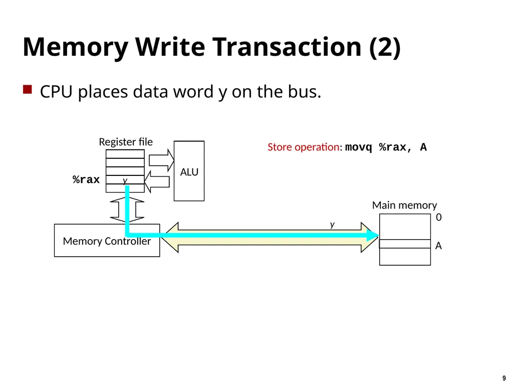
Memory Write Transaction (2) CPU places data word y on the bus. Register file Main memory 0 A %rax Store operation: movq %rax, A<br>
10
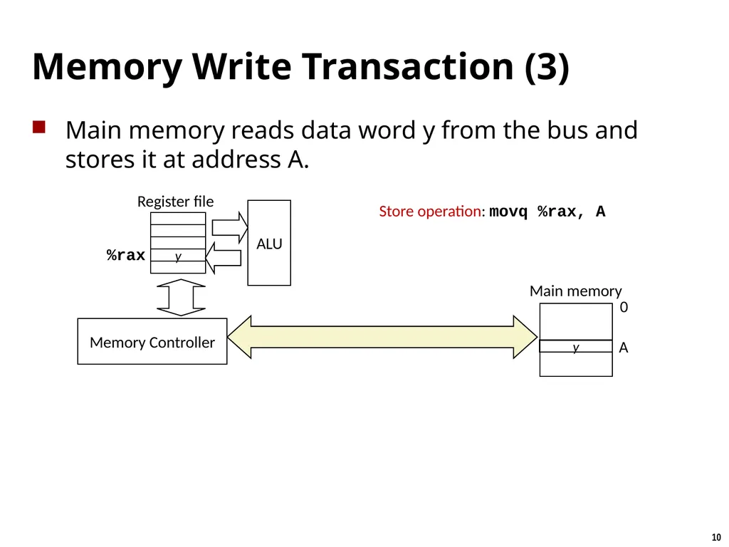
Memory Write Transaction (3) Main memory reads data word y from the bus and stores it at address A. Register file Main memory 0 A %rax Store operation: movq %rax, A<br>
11
The Memory Hierarchy The memory abstraction
Random-Access Memory (RAM): main memory building block
Locality of reference
The memory hierarchy
Storage technologies and trends<br>
Random-Access Memory (RAM): main memory building block
Locality of reference
The memory hierarchy
Storage technologies and trends<br>
12
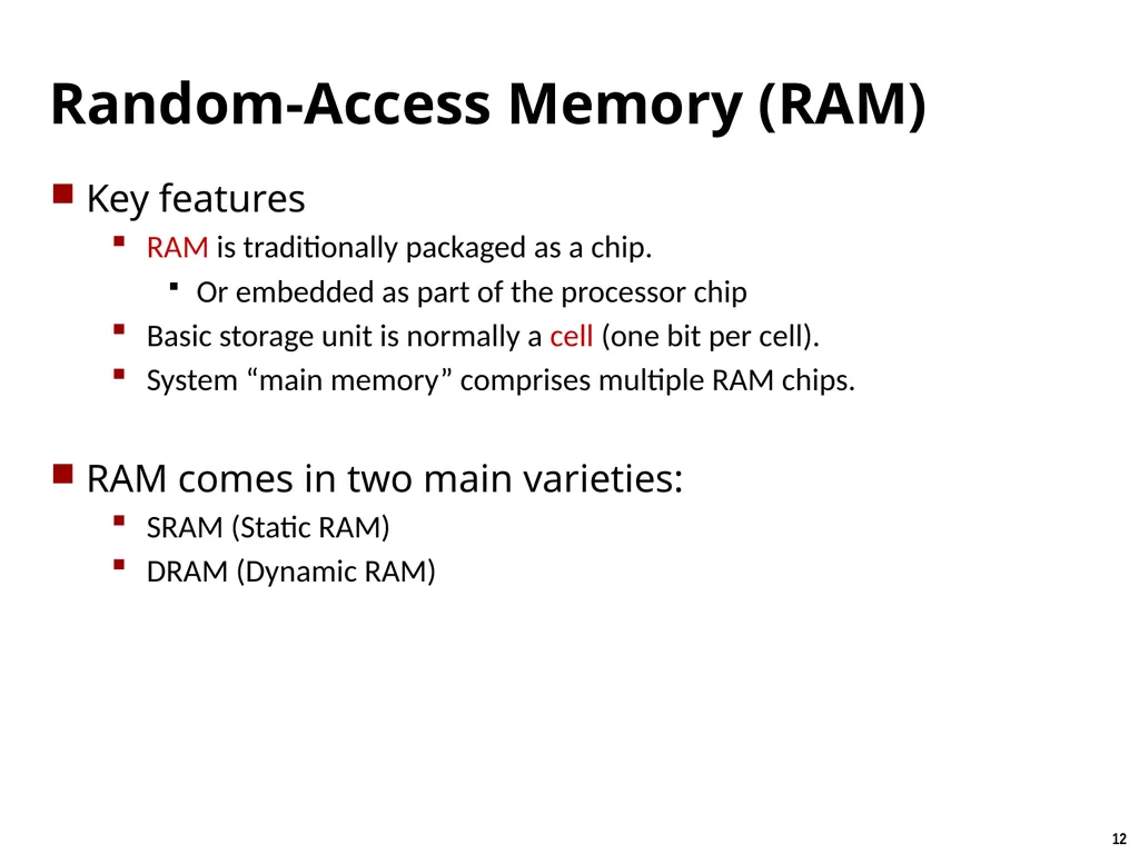
Random-Access Memory (RAM) Key features
RAM is traditionally packaged as a chip.
Or embedded as part of the processor chip
Basic storage unit is normally a cell (one bit per cell).
System “main memory” comprises multiple RAM chips.
RAM comes in two main varieties:
SRAM (Static RAM)
DRAM (Dynamic RAM)<br>
RAM is traditionally packaged as a chip.
Or embedded as part of the processor chip
Basic storage unit is normally a cell (one bit per cell).
System “main memory” comprises multiple RAM chips.
RAM comes in two main varieties:
SRAM (Static RAM)
DRAM (Dynamic RAM)<br>
13
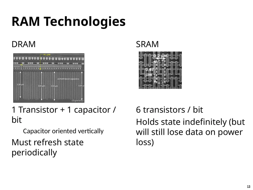
RAM Technologies DRAM
1 Transistor + 1 capacitor / bit
Capacitor oriented vertically
Must refresh state periodically SRAM
6 transistors / bit
Holds state indefinitely (but will still lose data on power loss)<br>
1 Transistor + 1 capacitor / bit
Capacitor oriented vertically
Must refresh state periodically SRAM
6 transistors / bit
Holds state indefinitely (but will still lose data on power loss)<br>
14
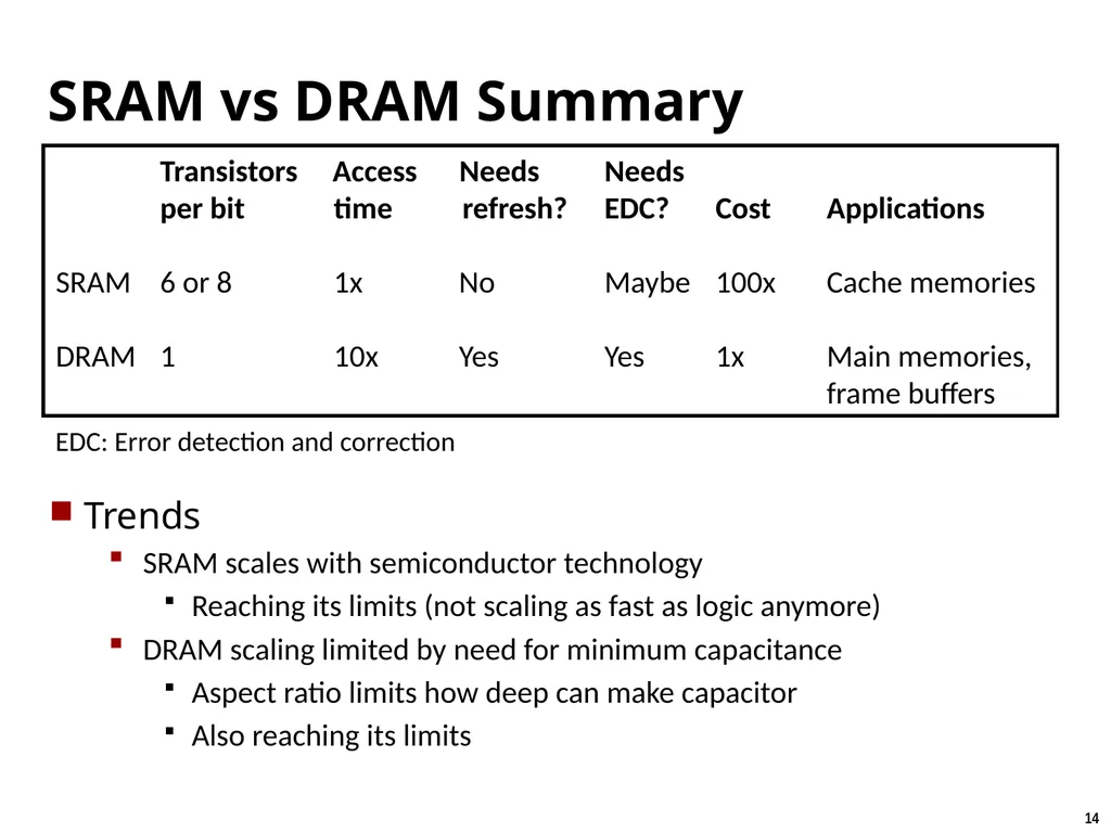
SRAM vs DRAM Summary Trends
SRAM scales with semiconductor technology
Reaching its limits (not scaling as fast as logic anymore)
DRAM scaling limited by need for minimum capacitance
Aspect ratio limits how deep can make capacitor
Also reaching its limits Transistors Access Needs Needs
per bit time refresh? EDC? Cost Applications
SRAM 6 or 8 1x No Maybe 100x Cache memories
DRAM 1 10x Yes Yes 1x Main memories,
frame buffers EDC: Error detection and correction<br>
SRAM scales with semiconductor technology
Reaching its limits (not scaling as fast as logic anymore)
DRAM scaling limited by need for minimum capacitance
Aspect ratio limits how deep can make capacitor
Also reaching its limits Transistors Access Needs Needs
per bit time refresh? EDC? Cost Applications
SRAM 6 or 8 1x No Maybe 100x Cache memories
DRAM 1 10x Yes Yes 1x Main memories,
frame buffers EDC: Error detection and correction<br>
15
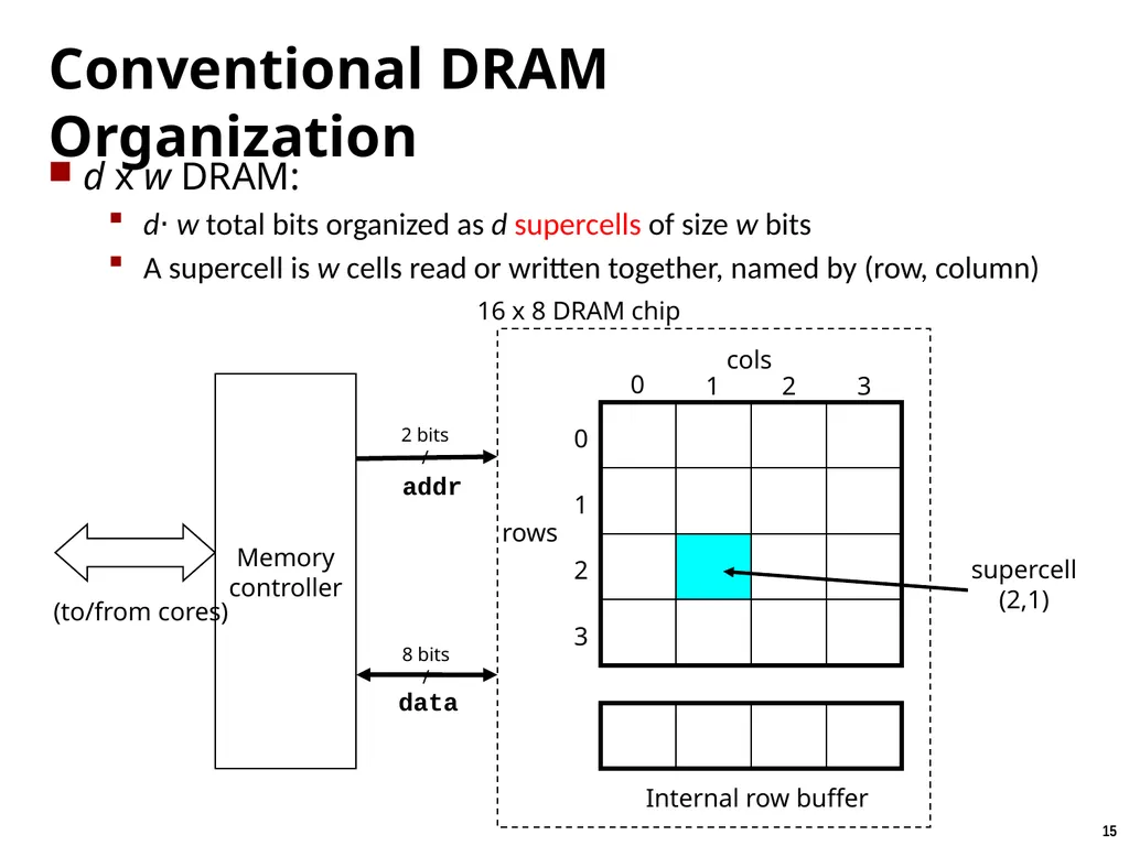
Conventional DRAM Organization d x w DRAM:
d⋅ w total bits organized as d supercells of size w bits
A supercell is w cells read or written together, named by (row, column) cols rows 0 1 2 3 0 1 2 3 Internal row buffer 16 x 8 DRAM chip addr data supercell
(2,1) 2 bits
/ 8 bits
/ (to/from cores)<br>
d⋅ w total bits organized as d supercells of size w bits
A supercell is w cells read or written together, named by (row, column) cols rows 0 1 2 3 0 1 2 3 Internal row buffer 16 x 8 DRAM chip addr data supercell
(2,1) 2 bits
/ 8 bits
/ (to/from cores)<br>
16
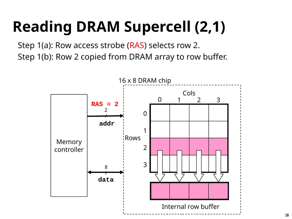
Reading DRAM Supercell (2,1) Step 1(a): Row access strobe (RAS) selects row 2.
Step 1(b): Row 2 copied from DRAM array to row buffer. Cols Rows RAS = 2 0 1 2 3 0 1 2 Internal row buffer 16 x 8 DRAM chip 3 addr data 2
/ 8
/<br>
Step 1(b): Row 2 copied from DRAM array to row buffer. Cols Rows RAS = 2 0 1 2 3 0 1 2 Internal row buffer 16 x 8 DRAM chip 3 addr data 2
/ 8
/<br>
17
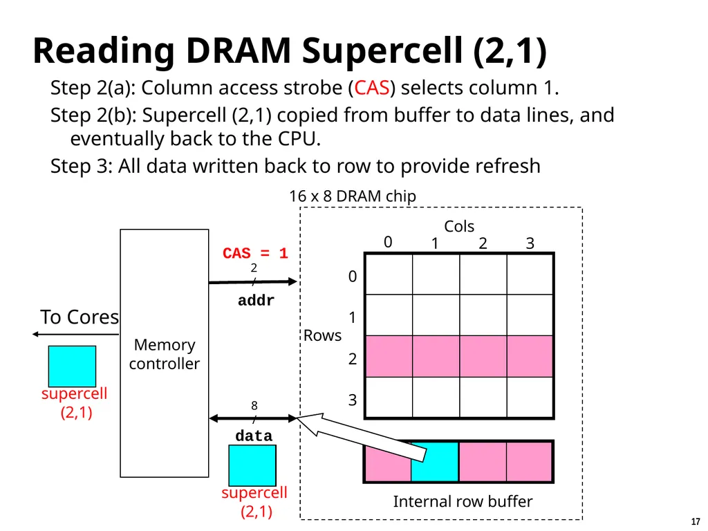
Reading DRAM Supercell (2,1) Step 2(a): Column access strobe (CAS) selects column 1.
Step 2(b): Supercell (2,1) copied from buffer to data lines, and eventually back to the CPU.
Step 3: All data written back to row to provide refresh Cols Rows 0 1 2 3 0 1 2 3 Internal row buffer 16 x 8 DRAM chip CAS = 1 addr data 2
/ 8
/<br>
Step 2(b): Supercell (2,1) copied from buffer to data lines, and eventually back to the CPU.
Step 3: All data written back to row to provide refresh Cols Rows 0 1 2 3 0 1 2 3 Internal row buffer 16 x 8 DRAM chip CAS = 1 addr data 2
/ 8
/<br>
18
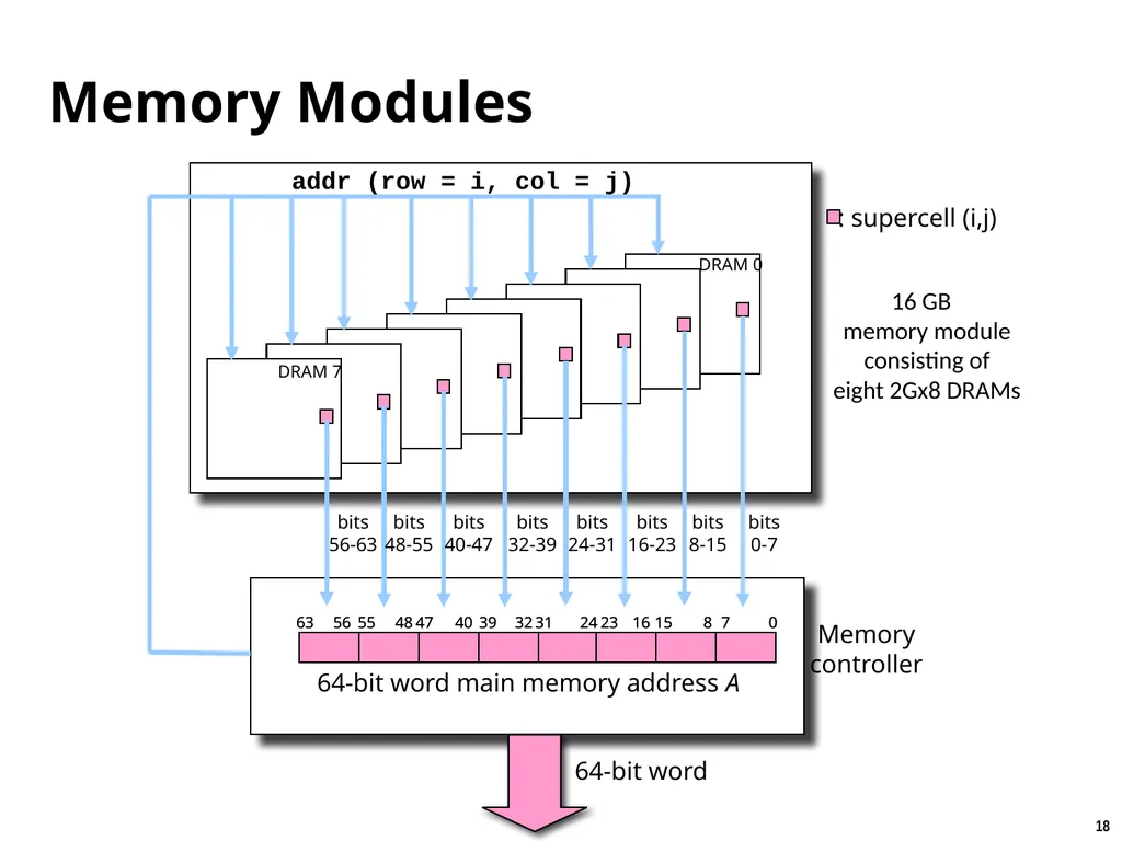
Memory Modules : supercell (i,j) 16 GB
memory module
consisting of
eight 2Gx8 DRAMs Memory
controller DRAM 7 DRAM 0<br>
memory module
consisting of
eight 2Gx8 DRAMs Memory
controller DRAM 7 DRAM 0<br>
19
Why a Write Sends the Address First In this model, address and data share the bus wires
Control lines say which one is on the bus
Only one can be there at a time, so the address goes first, then the data
Memory needs the address first
DRAM must select the right row and column before it can store the data
Sharing wires saves pins but costs time
DRAM chips do the same with row and column addresses (RAS, then CAS)
Real DDR memory has separate address and data pins
The data still follows the address by a fixed number of cycles
Caches (next lecture) change what memory sees
Whole 64-byte lines are written back, not each movq<br>
Control lines say which one is on the bus
Only one can be there at a time, so the address goes first, then the data
Memory needs the address first
DRAM must select the right row and column before it can store the data
Sharing wires saves pins but costs time
DRAM chips do the same with row and column addresses (RAS, then CAS)
Real DDR memory has separate address and data pins
The data still follows the address by a fixed number of cycles
Caches (next lecture) change what memory sees
Whole 64-byte lines are written back, not each movq<br>
20
The Memory Hierarchy The memory abstraction
Random-Access Memory (RAM): main memory building block
Locality of reference
The memory hierarchy
Storage technologies and trends<br>
Random-Access Memory (RAM): main memory building block
Locality of reference
The memory hierarchy
Storage technologies and trends<br>
21
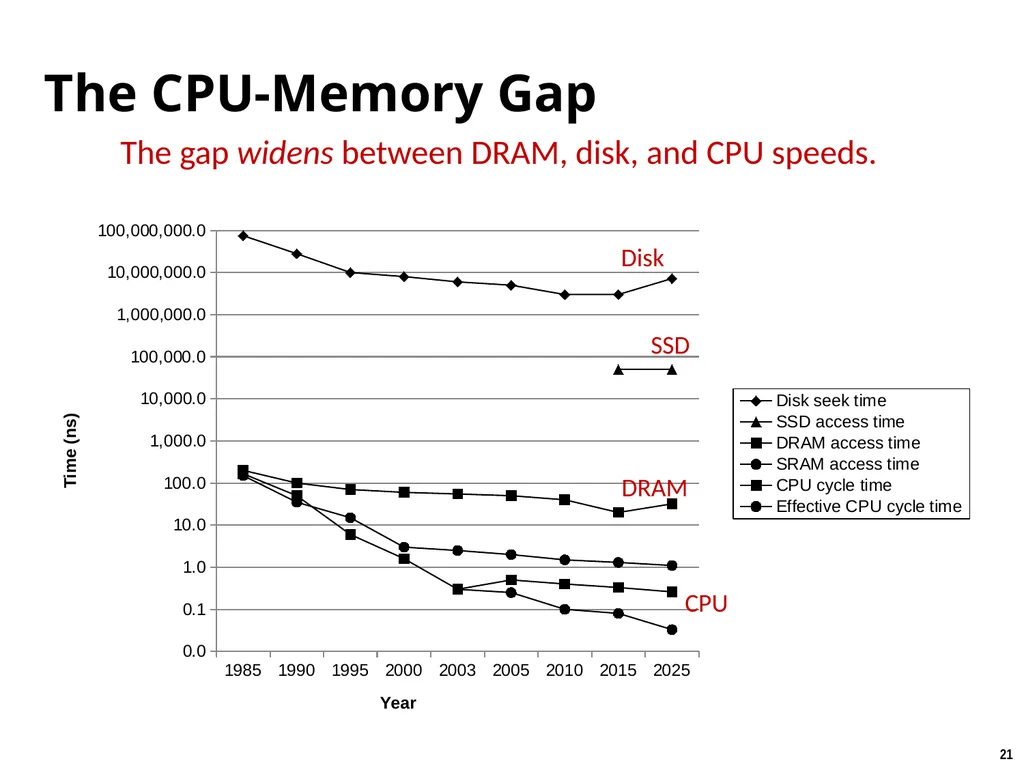
The CPU-Memory Gap The gap widens between DRAM, disk, and CPU speeds. DRAM CPU SSD Disk<br>
22
Locality to the Rescue! The key to bridging this CPU-Memory gap is an important property of computer programs known as locality.<br>
23
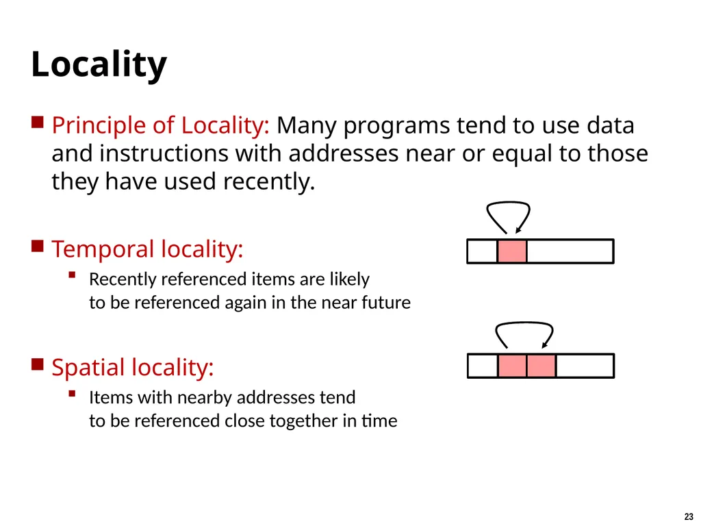
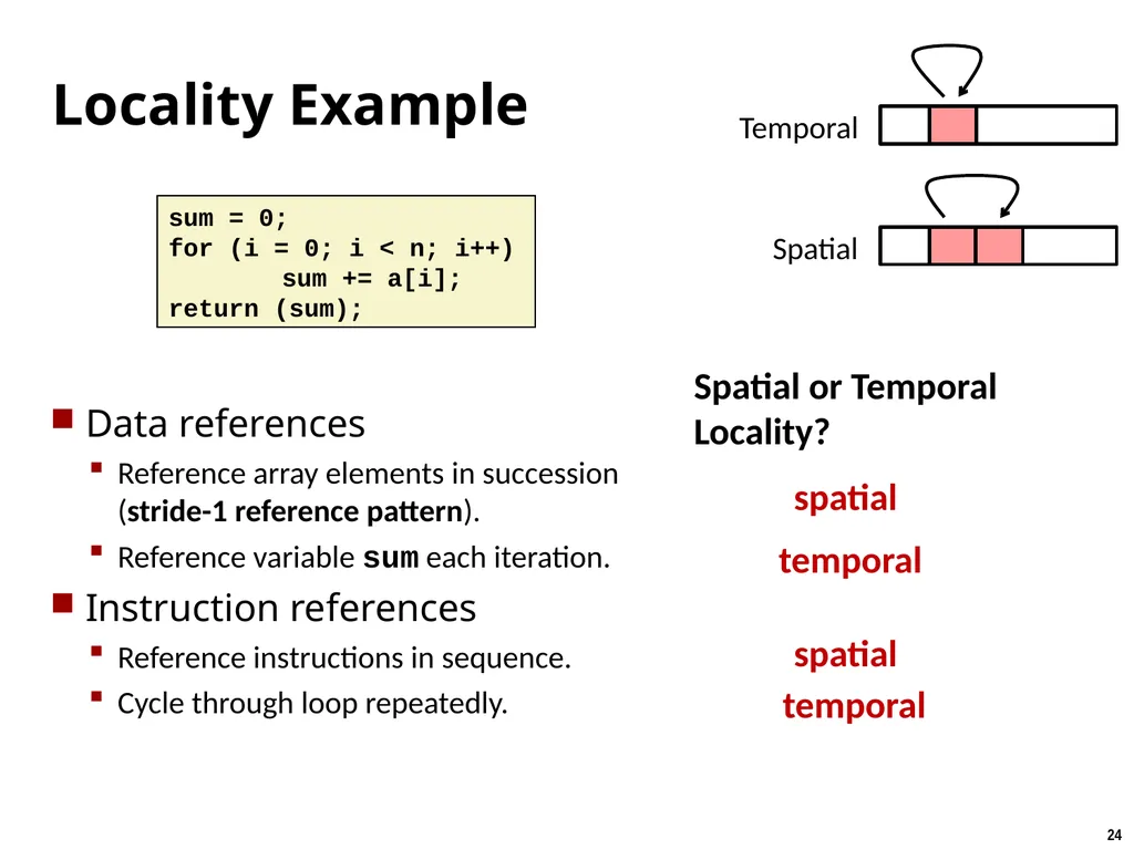
Locality Principle of Locality: Many programs tend to use data and instructions with addresses near or equal to those they have used recently.
Temporal locality:
Recently referenced items are likely to be referenced again in the near future
Spatial locality:
Items with nearby addresses tend to be referenced close together in time<br>
Temporal locality:
Recently referenced items are likely to be referenced again in the near future
Spatial locality:
Items with nearby addresses tend to be referenced close together in time<br>
24
Locality Example Data references
Reference array elements in succession (stride-1 reference pattern).
Reference variable sum each iteration.
Instruction references
Reference instructions in sequence.
Cycle through loop repeatedly. sum = 0;
for (i = 0; i < n; i++)
sum += a[i];
return (sum); Spatial or Temporal
Locality? temporal spatial temporal spatial Temporal Spatial<br>
Reference array elements in succession (stride-1 reference pattern).
Reference variable sum each iteration.
Instruction references
Reference instructions in sequence.
Cycle through loop repeatedly. sum = 0;
for (i = 0; i < n; i++)
sum += a[i];
return (sum); Spatial or Temporal
Locality? temporal spatial temporal spatial Temporal Spatial<br>
25
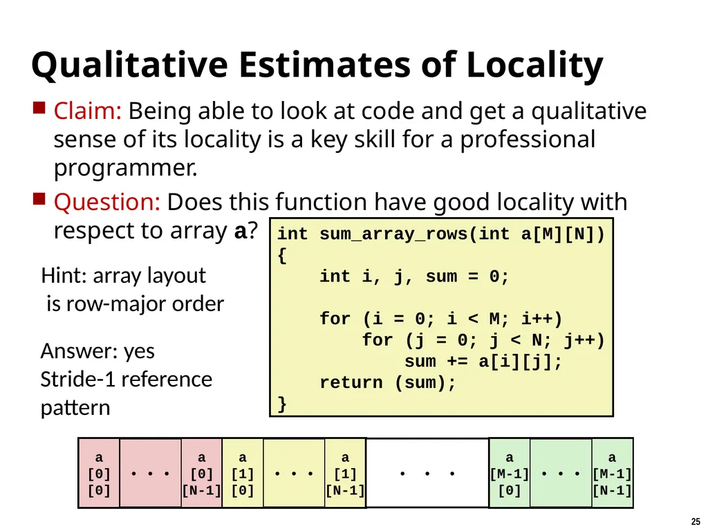
Qualitative Estimates of Locality Claim: Being able to look at code and get a qualitative sense of its locality is a key skill for a professional programmer.
Question: Does this function have good locality with respect to array a? int sum_array_rows(int a[M][N])
{
int i, j, sum = 0;
for (i = 0; i < M; i++)
for (j = 0; j < N; j++)
sum += a[i][j];
return (sum);
} Answer: yes
Stride-1 reference
pattern<br>
Question: Does this function have good locality with respect to array a? int sum_array_rows(int a[M][N])
{
int i, j, sum = 0;
for (i = 0; i < M; i++)
for (j = 0; j < N; j++)
sum += a[i][j];
return (sum);
} Answer: yes
Stride-1 reference
pattern<br>
26
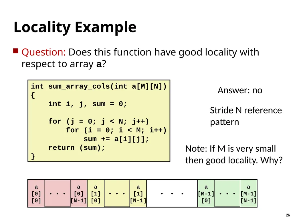
Locality Example Question: Does this function have good locality with respect to array a? int sum_array_cols(int a[M][N])
{
int i, j, sum = 0;
for (j = 0; j < N; j++)
for (i = 0; i < M; i++)
sum += a[i][j];
return (sum);
} Answer: no Stride N reference
pattern Note: If M is very small
then good locality. Why?<br>
{
int i, j, sum = 0;
for (j = 0; j < N; j++)
for (i = 0; i < M; i++)
sum += a[i][j];
return (sum);
} Answer: no Stride N reference
pattern Note: If M is very small
then good locality. Why?<br>
27
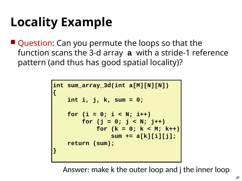
Locality Example Question: Can you permute the loops so that the function scans the 3-d array a with a stride-1 reference pattern (and thus has good spatial locality)? int sum_array_3d(int a[M][N][N])
{
int i, j, k, sum = 0;
for (i = 0; i < N; i++)
for (j = 0; j < N; j++)
for (k = 0; k < M; k++)
sum += a[k][i][j];
return (sum);
} Answer: make k the outer loop and j the inner loop<br>
{
int i, j, k, sum = 0;
for (i = 0; i < N; i++)
for (j = 0; j < N; j++)
for (k = 0; k < M; k++)
sum += a[k][i][j];
return (sum);
} Answer: make k the outer loop and j the inner loop<br>
28
The Memory Hierarchy The memory abstraction
Random-Access Memory (RAM): main memory building block
Locality of reference
The memory hierarchy
Storage technologies and trends<br>
Random-Access Memory (RAM): main memory building block
Locality of reference
The memory hierarchy
Storage technologies and trends<br>
29
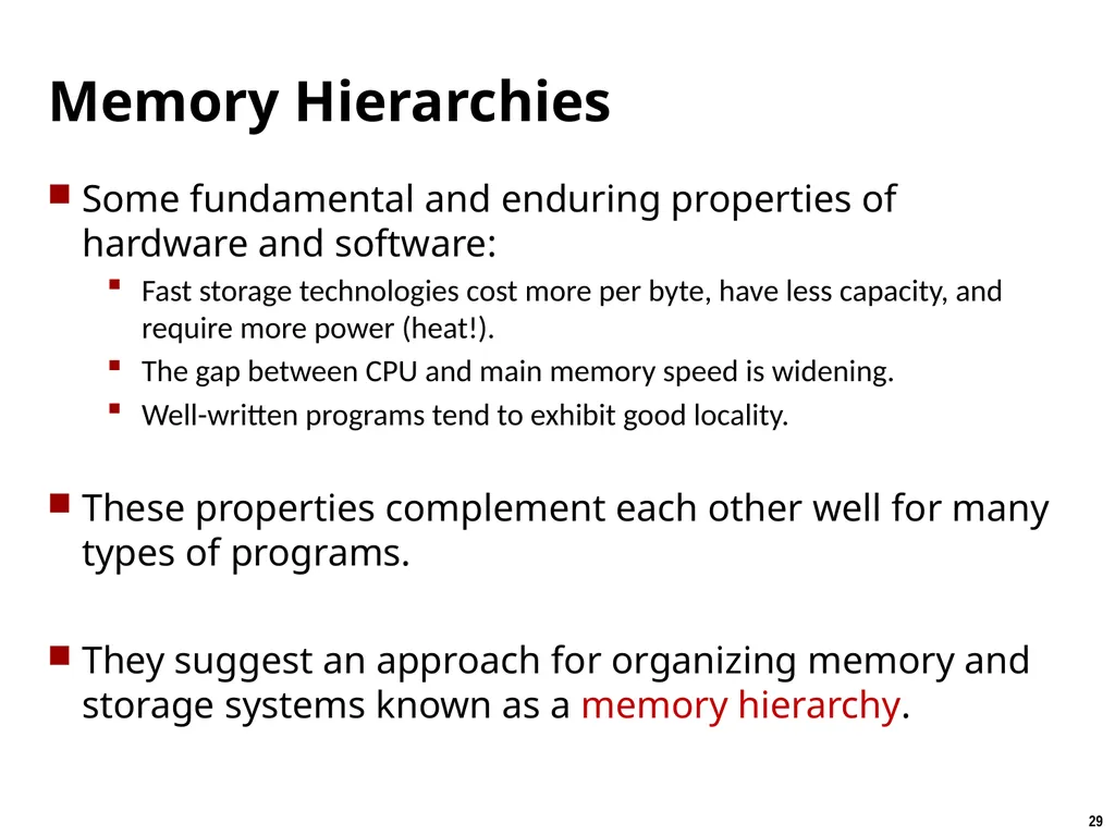
Memory Hierarchies Some fundamental and enduring properties of hardware and software:
Fast storage technologies cost more per byte, have less capacity, and require more power (heat!).
The gap between CPU and main memory speed is widening.
Well-written programs tend to exhibit good locality.
These properties complement each other well for many types of programs.
They suggest an approach for organizing memory and storage systems known as a memory hierarchy.<br>
Fast storage technologies cost more per byte, have less capacity, and require more power (heat!).
The gap between CPU and main memory speed is widening.
Well-written programs tend to exhibit good locality.
These properties complement each other well for many types of programs.
They suggest an approach for organizing memory and storage systems known as a memory hierarchy.<br>
30
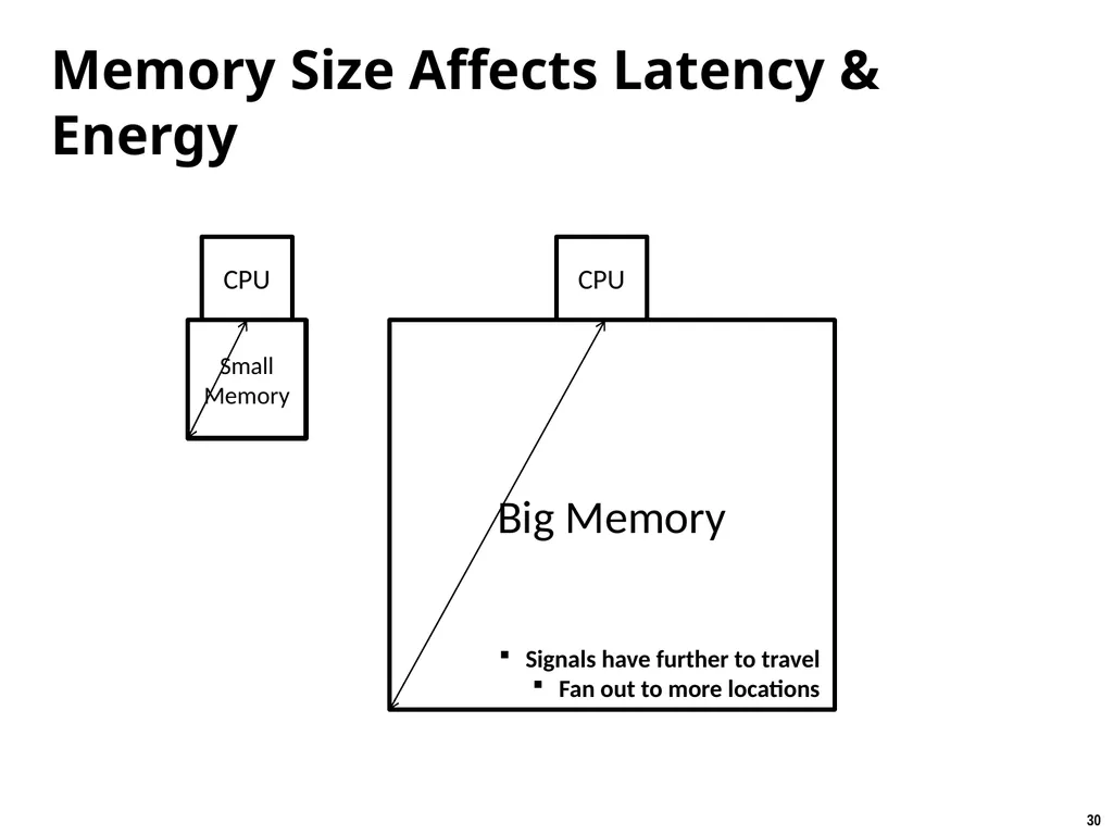
Memory Size Affects Latency & Energy Signals have further to travel
Fan out to more locations<br>
Fan out to more locations<br>
31
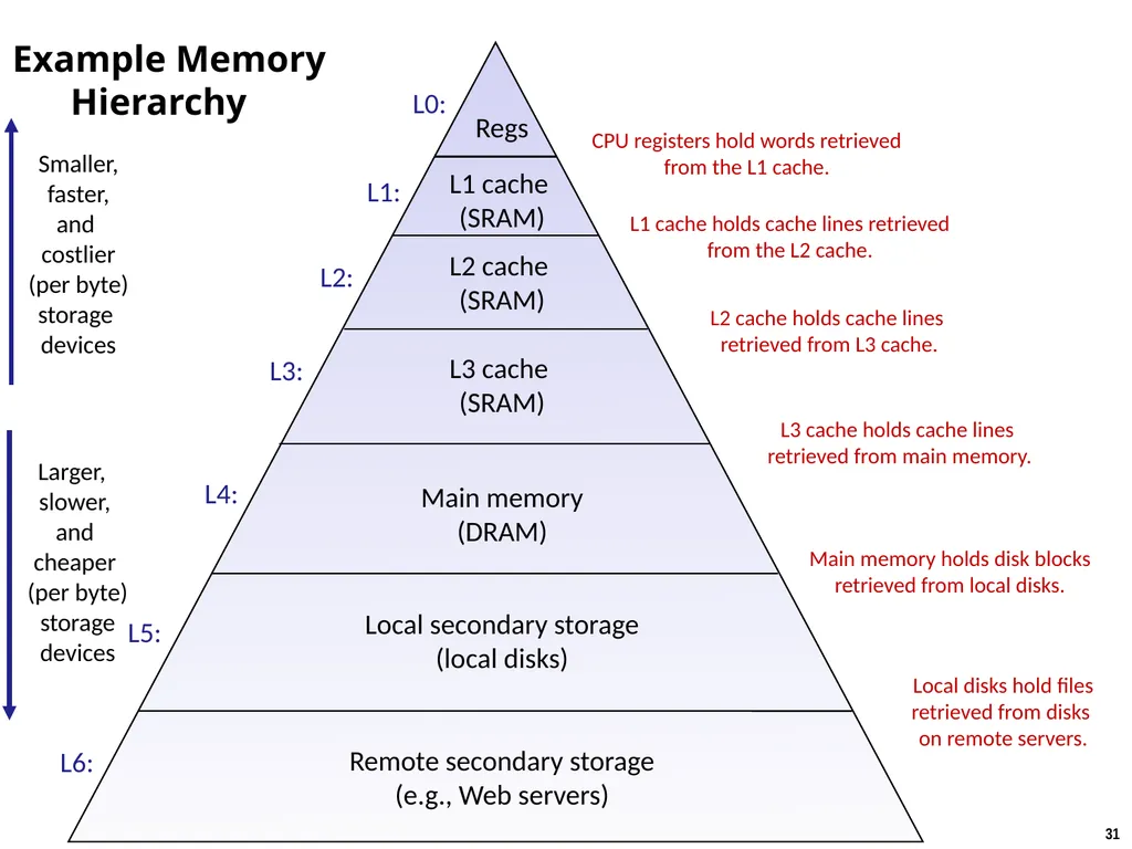
Example Memory
Hierarchy Regs L1 cache
(SRAM) Main memory
(DRAM) Local secondary storage
(local disks) Larger,
slower,
and
cheaper
(per byte)
storage
devices Remote secondary storage
(e.g., Web servers) Local disks hold files retrieved from disks
on remote servers. L2 cache
(SRAM) L1 cache holds cache lines retrieved from the L2 cache. CPU registers hold words retrieved from the L1 cache. L2 cache holds cache lines
retrieved from L3 cache. L0: L1: L2: L3: L4: L5: Smaller,
faster,
and
costlier
(per byte)
storage
devices L3 cache
(SRAM) L3 cache holds cache lines
retrieved from main memory. L6: Main memory holds disk blocks retrieved from local disks.<br>
(SRAM) Main memory
(DRAM) Local secondary storage
(local disks) Larger,
slower,
and
cheaper
(per byte)
storage
devices Remote secondary storage
(e.g., Web servers) Local disks hold files retrieved from disks
on remote servers. L2 cache
(SRAM) L1 cache holds cache lines retrieved from the L2 cache. CPU registers hold words retrieved from the L1 cache. L2 cache holds cache lines
retrieved from L3 cache. L0: L1: L2: L3: L4: L5: Smaller,
faster,
and
costlier
(per byte)
storage
devices L3 cache
(SRAM) L3 cache holds cache lines
retrieved from main memory. L6: Main memory holds disk blocks retrieved from local disks.<br>
32
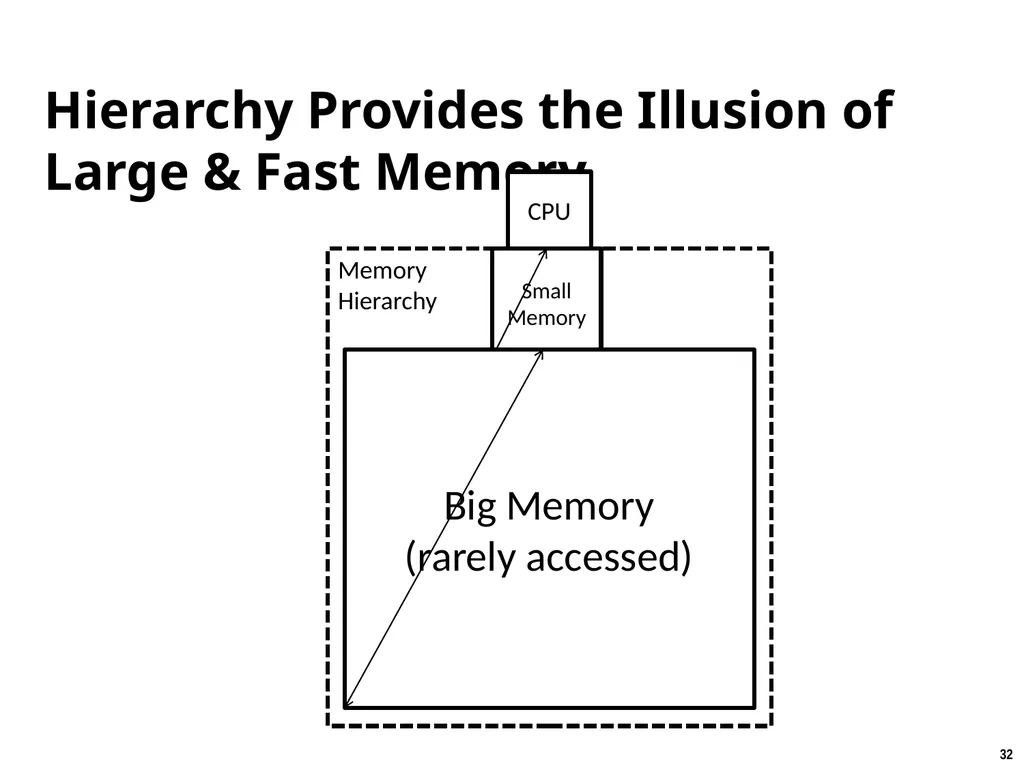
Hierarchy Provides the Illusion of Large & Fast Memory Big Memory
(rarely accessed) CPU Memory
Hierarchy<br>
33
Caches Cache: A smaller, faster storage device that acts as a staging area for a subset of the data in a larger, slower device.
Fundamental idea of a memory hierarchy:
For each k, the faster, smaller device at level k serves as a cache for the larger, slower device at level k+1.
Why do memory hierarchies work?
Because of locality: programs tend to access the data at level k more often than they access the data at level k+1.
Thus, the storage at level k+1 can be slower, and thus larger and cheaper per bit.
Big Idea (Ideal): The memory hierarchy creates a large pool of storage that costs as much as the cheap storage near the bottom, but that serves data to programs at the rate of the fast storage near the top.<br>
Fundamental idea of a memory hierarchy:
For each k, the faster, smaller device at level k serves as a cache for the larger, slower device at level k+1.
Why do memory hierarchies work?
Because of locality: programs tend to access the data at level k more often than they access the data at level k+1.
Thus, the storage at level k+1 can be slower, and thus larger and cheaper per bit.
Big Idea (Ideal): The memory hierarchy creates a large pool of storage that costs as much as the cheap storage near the bottom, but that serves data to programs at the rate of the fast storage near the top.<br>
34
Cache versus Memory Caches are invisible (transparent) to software
Managed by hardware in response to loads & stores
Performance & energy improve without software changes
Caveat: Recent CPUs have some instructions to manage cache (e.g., prefetch, invalidate, partition…)
Memory is visible to software
I.e., addressable directly by instructions (memory address, registers)
Some optimization opportunities, but only w/ software changes<br>
Managed by hardware in response to loads & stores
Performance & energy improve without software changes
Caveat: Recent CPUs have some instructions to manage cache (e.g., prefetch, invalidate, partition…)
Memory is visible to software
I.e., addressable directly by instructions (memory address, registers)
Some optimization opportunities, but only w/ software changes<br>
35
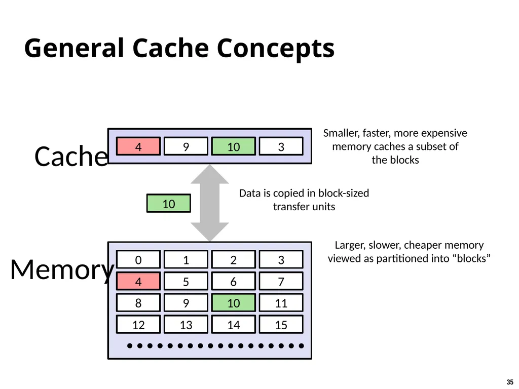
General Cache Concepts Cache Memory Larger, slower, cheaper memory
viewed as partitioned into “blocks” Data is copied in block-sized transfer units Smaller, faster, more expensive
memory caches a subset of
the blocks<br>
viewed as partitioned into “blocks” Data is copied in block-sized transfer units Smaller, faster, more expensive
memory caches a subset of
the blocks<br>
36
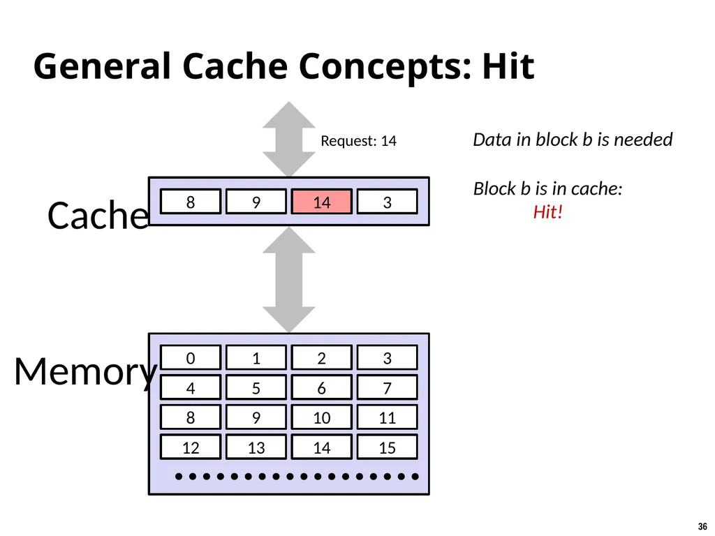
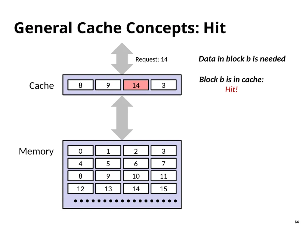
General Cache Concepts: Hit Cache Memory Data in block b is needed Request: 14 Block b is in cache:
Hit!<br>
Hit!<br>
37
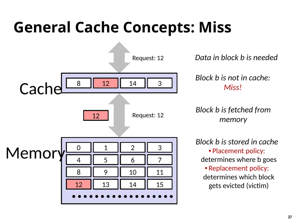
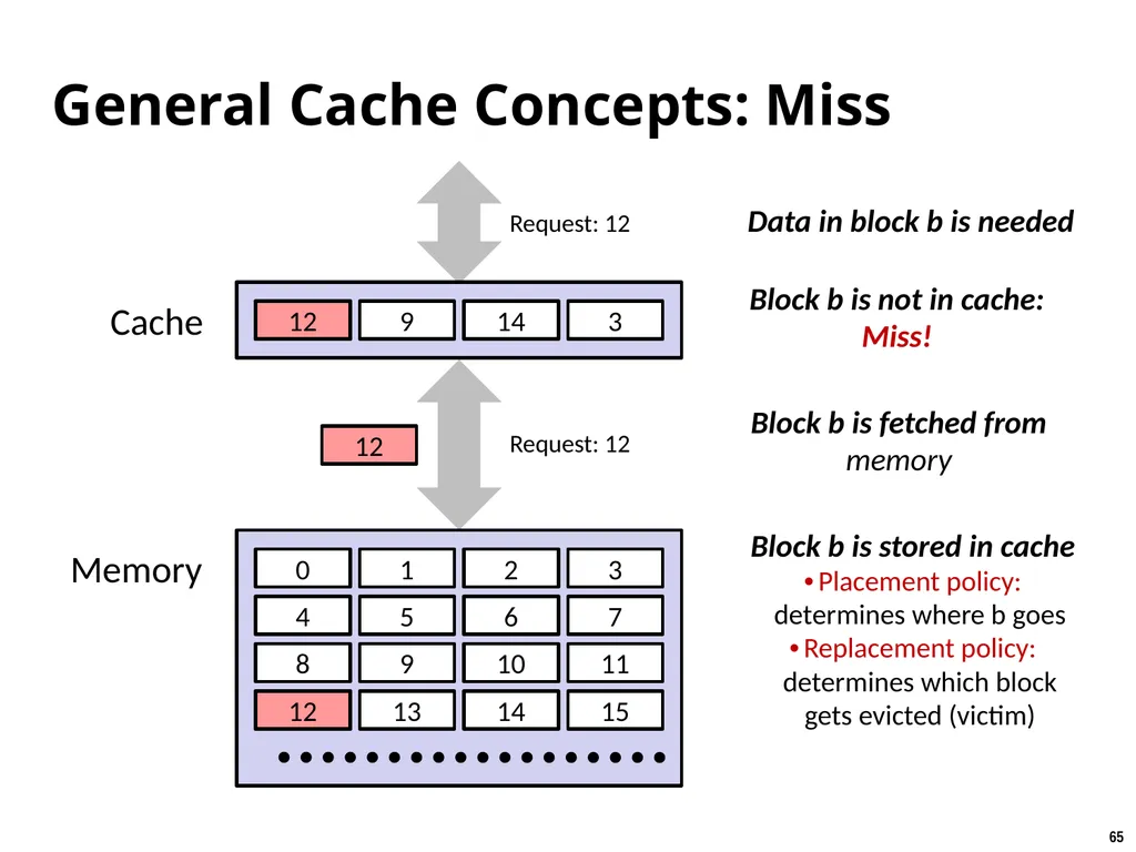
General Cache Concepts: Miss Cache Memory Data in block b is needed Request: 12 Block b is not in cache:
Miss! Block b is fetched from
memory Request: 12 Block b is stored in cache
Placement policy: determines where b goes
Replacement policy: determines which block gets evicted (victim)<br>
Miss! Block b is fetched from
memory Request: 12 Block b is stored in cache
Placement policy: determines where b goes
Replacement policy: determines which block gets evicted (victim)<br>
38
General Caching Concepts:
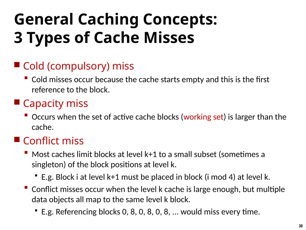
3 Types of Cache Misses Cold (compulsory) miss
Cold misses occur because the cache starts empty and this is the first reference to the block.
Capacity miss
Occurs when the set of active cache blocks (working set) is larger than the cache.
Conflict miss
Most caches limit blocks at level k+1 to a small subset (sometimes a singleton) of the block positions at level k.
E.g. Block i at level k+1 must be placed in block (i mod 4) at level k.
Conflict misses occur when the level k cache is large enough, but multiple data objects all map to the same level k block.
E.g. Referencing blocks 0, 8, 0, 8, 0, 8, ... would miss every time.<br>
Cold misses occur because the cache starts empty and this is the first reference to the block.
Capacity miss
Occurs when the set of active cache blocks (working set) is larger than the cache.
Conflict miss
Most caches limit blocks at level k+1 to a small subset (sometimes a singleton) of the block positions at level k.
E.g. Block i at level k+1 must be placed in block (i mod 4) at level k.
Conflict misses occur when the level k cache is large enough, but multiple data objects all map to the same level k block.
E.g. Referencing blocks 0, 8, 0, 8, 0, 8, ... would miss every time.<br>
39
General Caching Concepts:
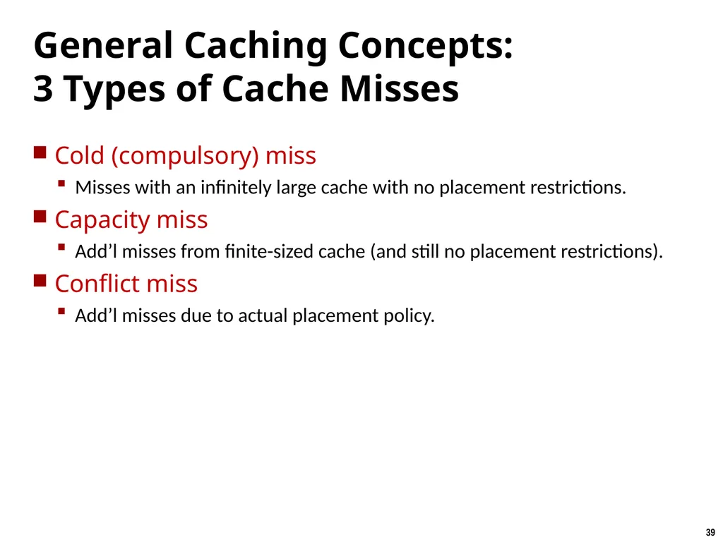
3 Types of Cache Misses Cold (compulsory) miss
Misses with an infinitely large cache with no placement restrictions.
Capacity miss
Add’l misses from finite-sized cache (and still no placement restrictions).
Conflict miss
Add’l misses due to actual placement policy.<br>
Misses with an infinitely large cache with no placement restrictions.
Capacity miss
Add’l misses from finite-sized cache (and still no placement restrictions).
Conflict miss
Add’l misses due to actual placement policy.<br>
40
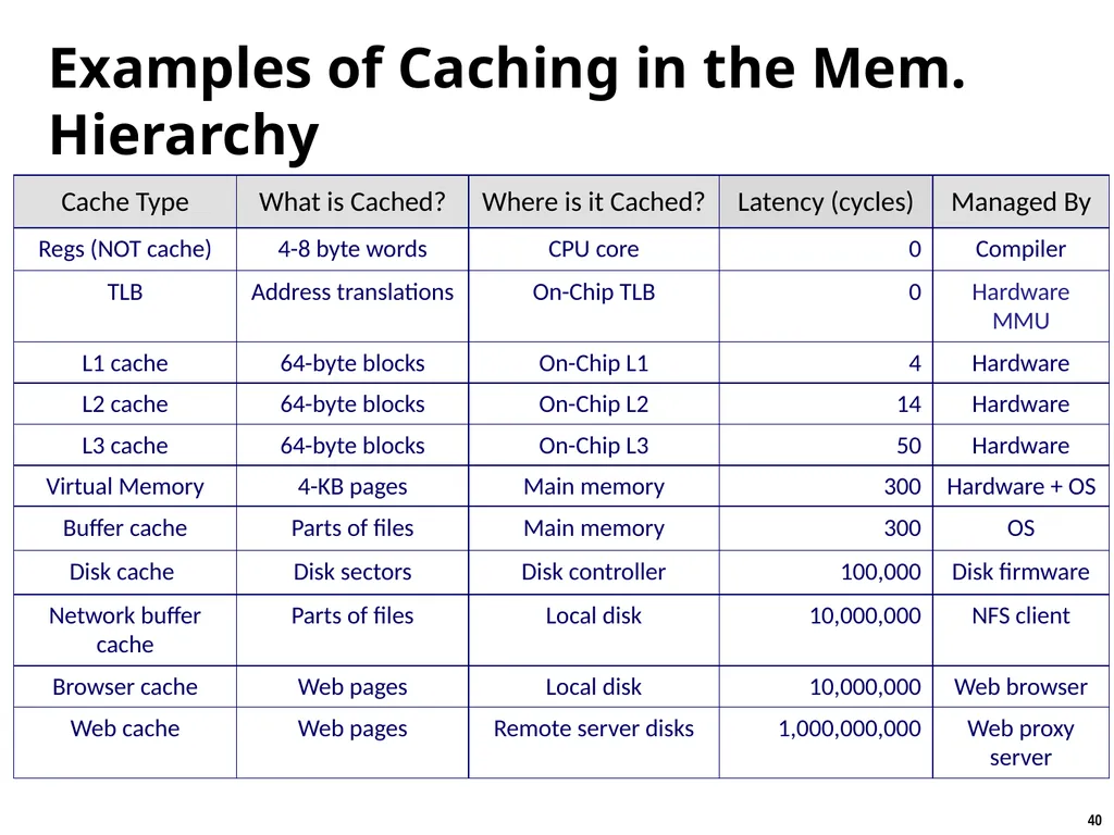
Examples of Caching in the Mem. Hierarchy<br>
41
The Memory Hierarchy The memory abstraction
Random-Access Memory (RAM): main memory building block
Locality of reference
The memory hierarchy
Storage technologies and trends<br>
Random-Access Memory (RAM): main memory building block
Locality of reference
The memory hierarchy
Storage technologies and trends<br>
42
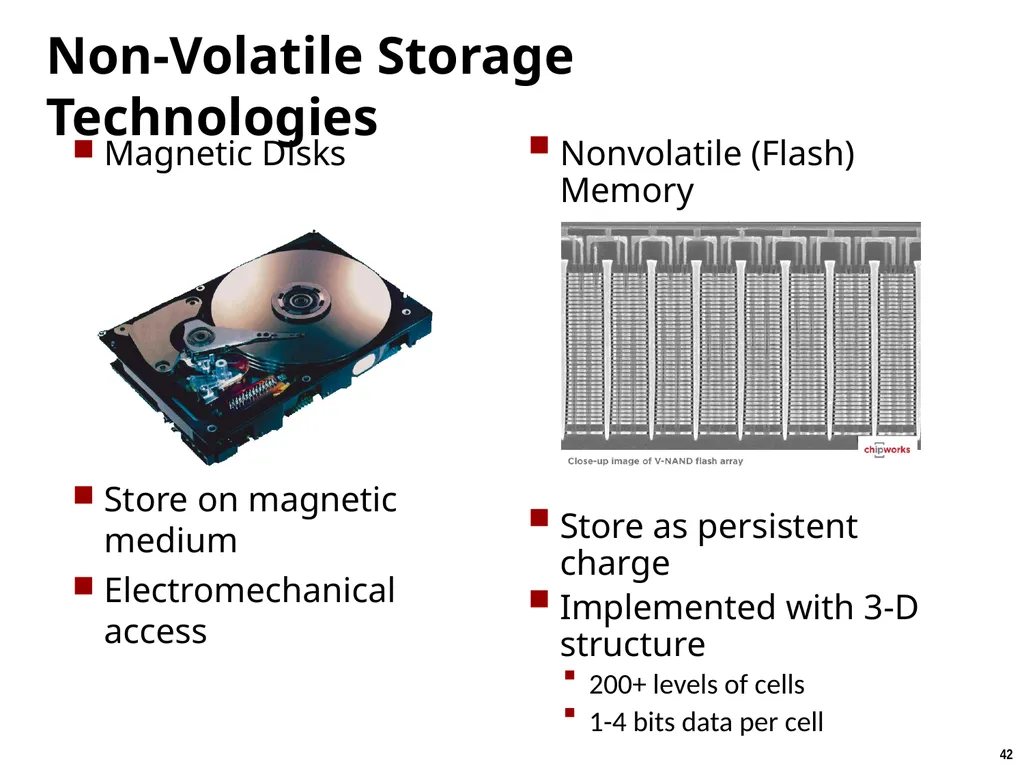
Non-Volatile Storage Technologies Magnetic Disks
Store on magnetic medium
Electromechanical access Nonvolatile (Flash) Memory
Store as persistent charge
Implemented with 3-D structure
200+ levels of cells
1-4 bits data per cell<br>
Store on magnetic medium
Electromechanical access Nonvolatile (Flash) Memory
Store as persistent charge
Implemented with 3-D structure
200+ levels of cells
1-4 bits data per cell<br>
43
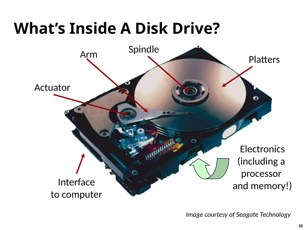
What’s Inside A Disk Drive? Spindle Arm Actuator Platters Electronics
(including a
processor
and memory!) Interface
to computer Image courtesy of Seagate Technology<br>
(including a
processor
and memory!) Interface
to computer Image courtesy of Seagate Technology<br>
44
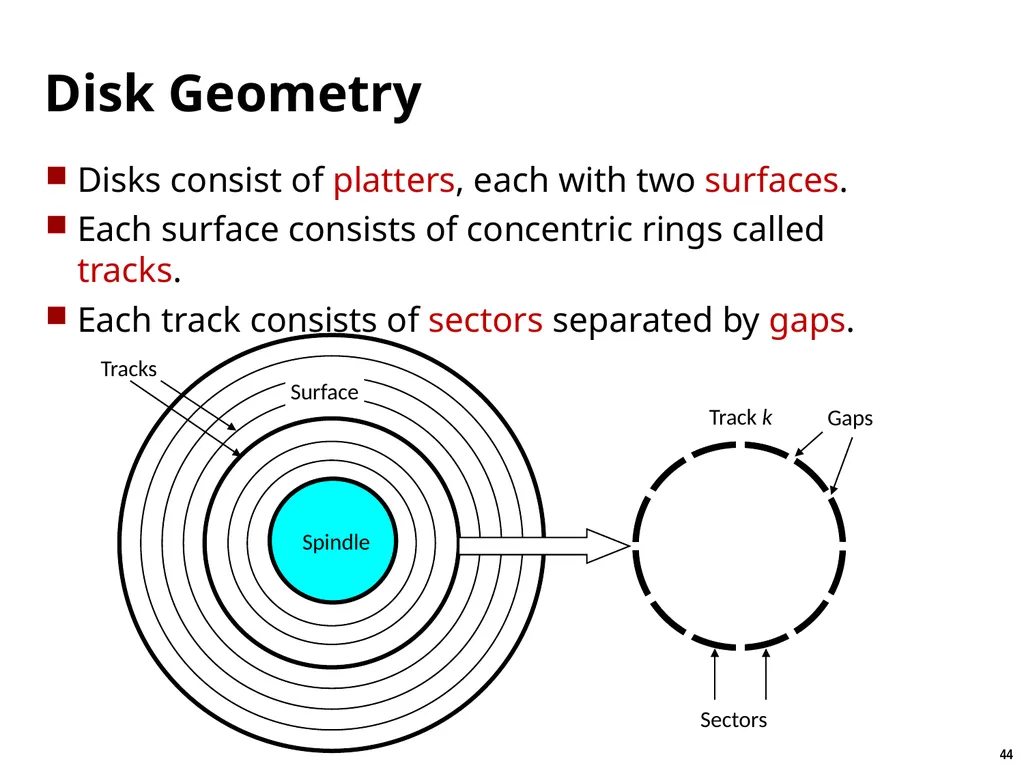
Disk Geometry Disks consist of platters, each with two surfaces.
Each surface consists of concentric rings called tracks.
Each track consists of sectors separated by gaps. Surface Tracks Track k Sectors Gaps<br>
Each surface consists of concentric rings called tracks.
Each track consists of sectors separated by gaps. Surface Tracks Track k Sectors Gaps<br>
45
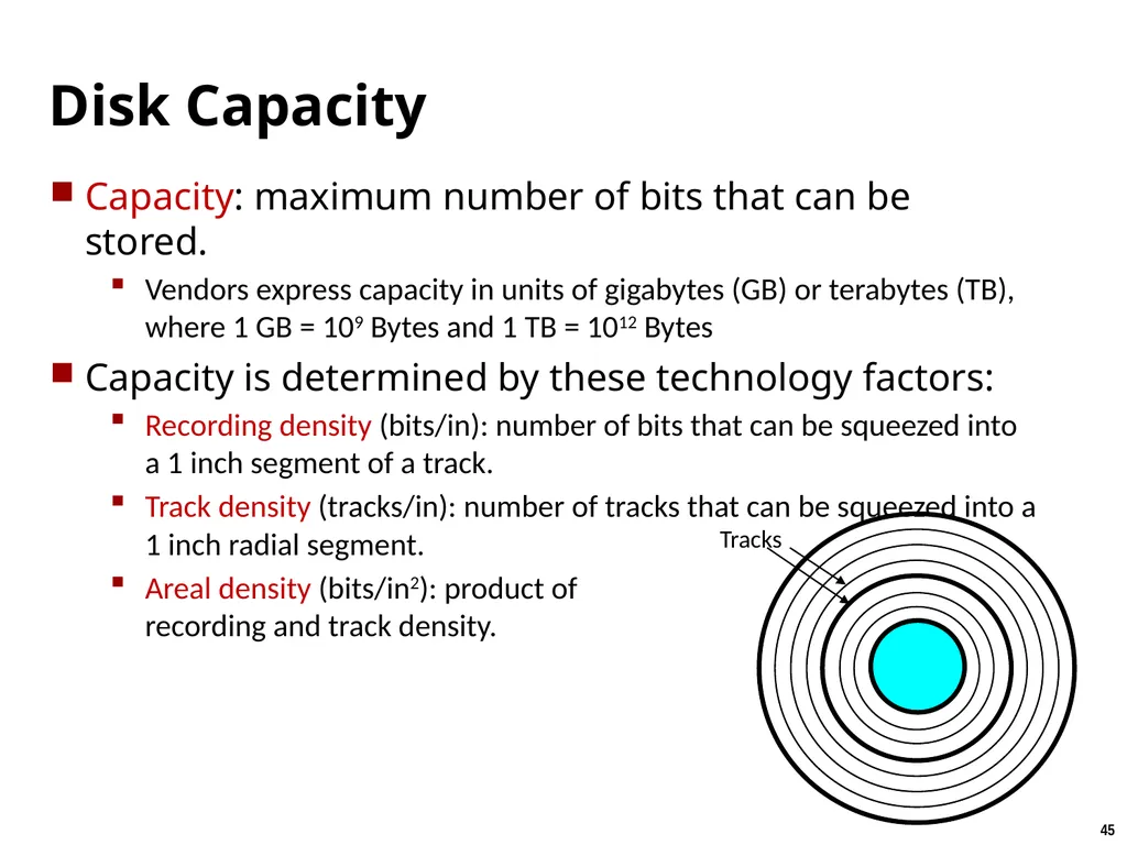
Disk Capacity Capacity: maximum number of bits that can be stored.
Vendors express capacity in units of gigabytes (GB) or terabytes (TB), where 1 GB = 109 Bytes and 1 TB = 1012 Bytes
Capacity is determined by these technology factors:
Recording density (bits/in): number of bits that can be squeezed into a 1 inch segment of a track.
Track density (tracks/in): number of tracks that can be squeezed into a 1 inch radial segment.
Areal density (bits/in2): product of recording and track density.<br>
Vendors express capacity in units of gigabytes (GB) or terabytes (TB), where 1 GB = 109 Bytes and 1 TB = 1012 Bytes
Capacity is determined by these technology factors:
Recording density (bits/in): number of bits that can be squeezed into a 1 inch segment of a track.
Track density (tracks/in): number of tracks that can be squeezed into a 1 inch radial segment.
Areal density (bits/in2): product of recording and track density.<br>
46
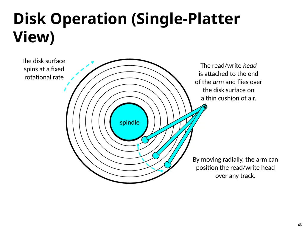
Disk Operation (Single-Platter View) The disk surface
spins at a fixed
rotational rate<br>
spins at a fixed
rotational rate<br>
47
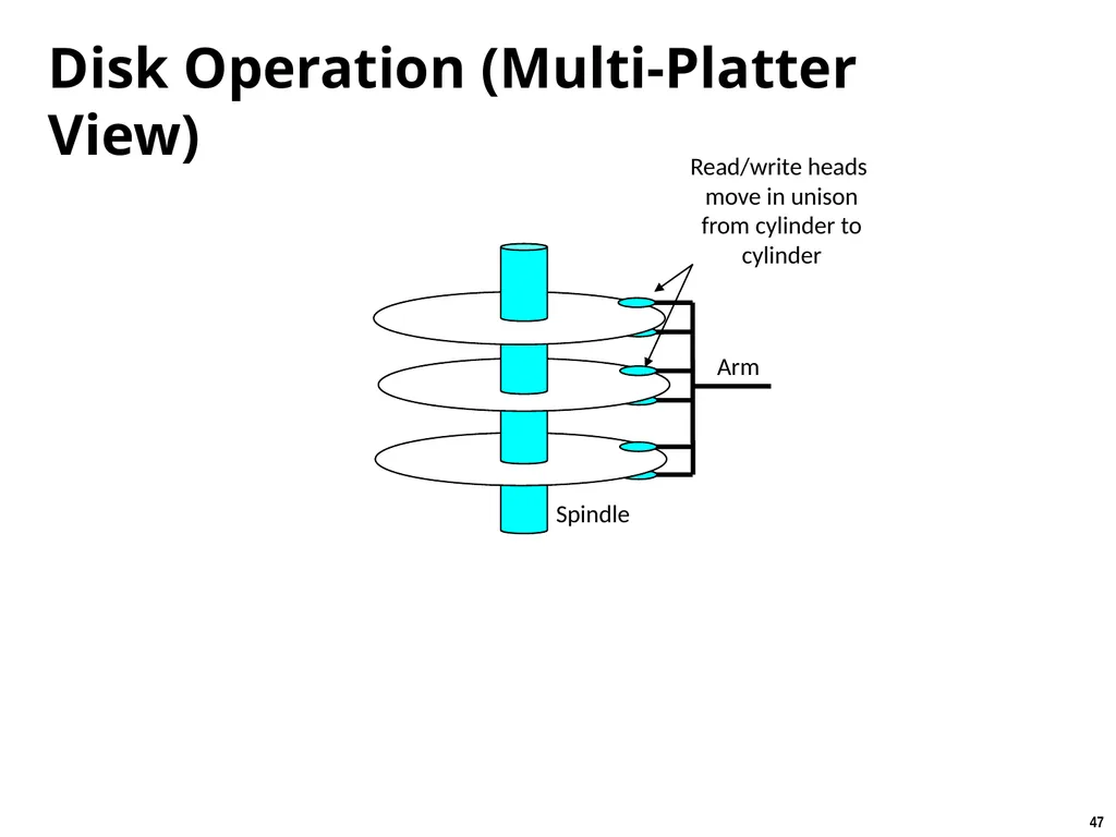
Disk Operation (Multi-Platter View) Arm Read/write heads
move in unison
from cylinder to cylinder Spindle<br>
move in unison
from cylinder to cylinder Spindle<br>
48
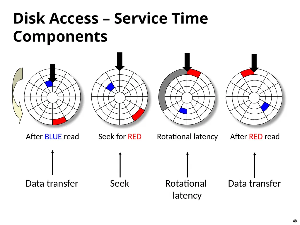
Disk Access – Service Time Components After BLUE read Seek for RED Rotational latency After RED read Data transfer Seek Rotational
latency Data transfer<br>
latency Data transfer<br>
49
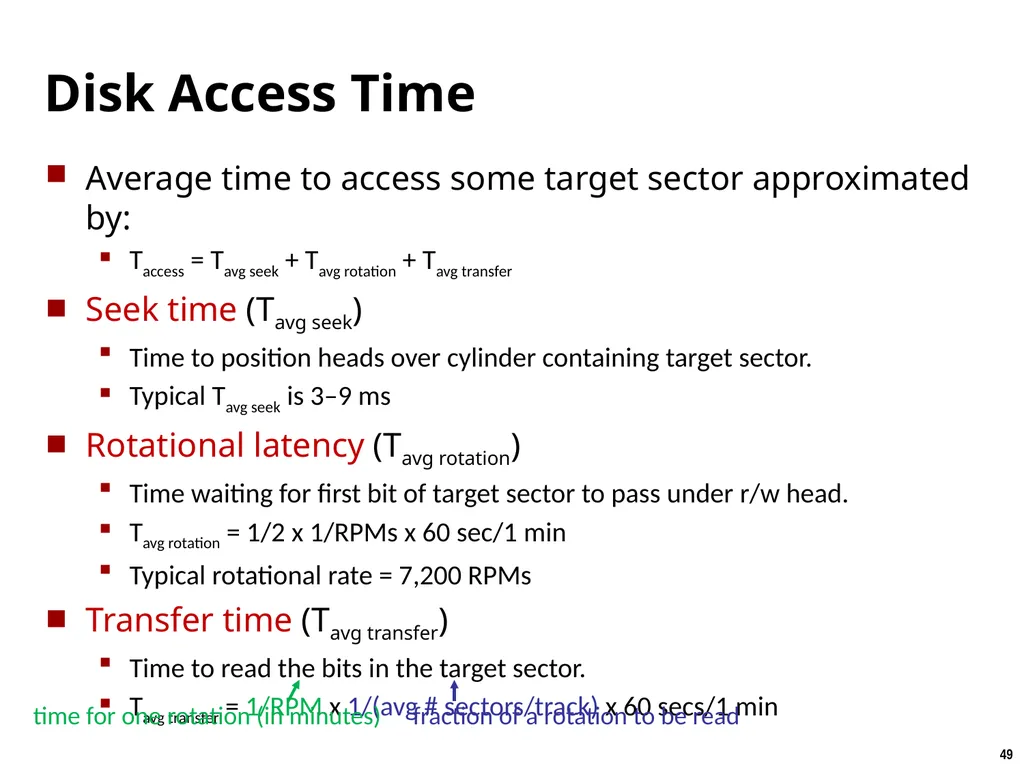
Disk Access Time Average time to access some target sector approximated by:
Taccess = Tavg seek + Tavg rotation + Tavg transfer
Seek time (Tavg seek)
Time to position heads over cylinder containing target sector.
Typical Tavg seek is 3–9 ms
Rotational latency (Tavg rotation)
Time waiting for first bit of target sector to pass under r/w head.
Tavg rotation = 1/2 x 1/RPMs x 60 sec/1 min
Typical rotational rate = 7,200 RPMs
Transfer time (Tavg transfer)
Time to read the bits in the target sector.
Tavg transfer = 1/RPM x 1/(avg # sectors/track) x 60 secs/1 min time for one rotation (in minutes) fraction of a rotation to be read<br>
Taccess = Tavg seek + Tavg rotation + Tavg transfer
Seek time (Tavg seek)
Time to position heads over cylinder containing target sector.
Typical Tavg seek is 3–9 ms
Rotational latency (Tavg rotation)
Time waiting for first bit of target sector to pass under r/w head.
Tavg rotation = 1/2 x 1/RPMs x 60 sec/1 min
Typical rotational rate = 7,200 RPMs
Transfer time (Tavg transfer)
Time to read the bits in the target sector.
Tavg transfer = 1/RPM x 1/(avg # sectors/track) x 60 secs/1 min time for one rotation (in minutes) fraction of a rotation to be read<br>
50
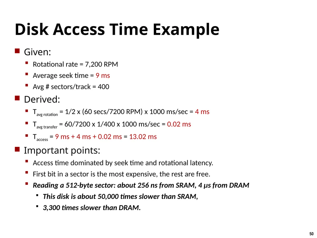
Disk Access Time Example Given:
Rotational rate = 7,200 RPM
Average seek time = 9 ms
Avg # sectors/track = 400
Derived:
Tavg rotation = 1/2 x (60 secs/7200 RPM) x 1000 ms/sec = 4 ms
Tavg transfer = 60/7200 x 1/400 x 1000 ms/sec = 0.02 ms
Taccess = 9 ms + 4 ms + 0.02 ms = 13.02 ms
Important points:
Access time dominated by seek time and rotational latency.
First bit in a sector is the most expensive, the rest are free.
Reading a 512-byte sector: about 256 ns from SRAM, 4 µs from DRAM
This disk is about 50,000 times slower than SRAM,
3,300 times slower than DRAM.<br>
Rotational rate = 7,200 RPM
Average seek time = 9 ms
Avg # sectors/track = 400
Derived:
Tavg rotation = 1/2 x (60 secs/7200 RPM) x 1000 ms/sec = 4 ms
Tavg transfer = 60/7200 x 1/400 x 1000 ms/sec = 0.02 ms
Taccess = 9 ms + 4 ms + 0.02 ms = 13.02 ms
Important points:
Access time dominated by seek time and rotational latency.
First bit in a sector is the most expensive, the rest are free.
Reading a 512-byte sector: about 256 ns from SRAM, 4 µs from DRAM
This disk is about 50,000 times slower than SRAM,
3,300 times slower than DRAM.<br>
51
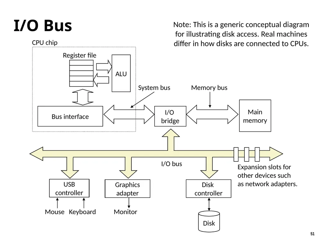
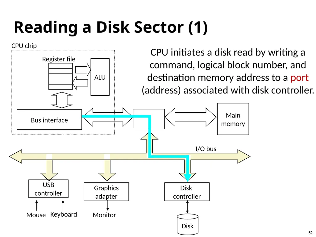
I/O Bus Main
memory I/O
bridge Bus interface ALU Register file CPU chip System bus Memory bus Disk
controller Graphics
adapter USB
controller Mouse Keyboard Monitor Disk I/O bus Expansion slots for
other devices such
as network adapters. Note: This is a generic conceptual diagram
for illustrating disk access. Real machines differ in how disks are connected to CPUs.<br>
memory I/O
bridge Bus interface ALU Register file CPU chip System bus Memory bus Disk
controller Graphics
adapter USB
controller Mouse Keyboard Monitor Disk I/O bus Expansion slots for
other devices such
as network adapters. Note: This is a generic conceptual diagram
for illustrating disk access. Real machines differ in how disks are connected to CPUs.<br>
52
Reading a Disk Sector (1) Register file CPU chip Mouse Keyboard Monitor I/O bus CPU initiates a disk read by writing a command, logical block number, and destination memory address to a port (address) associated with disk controller.<br>
53
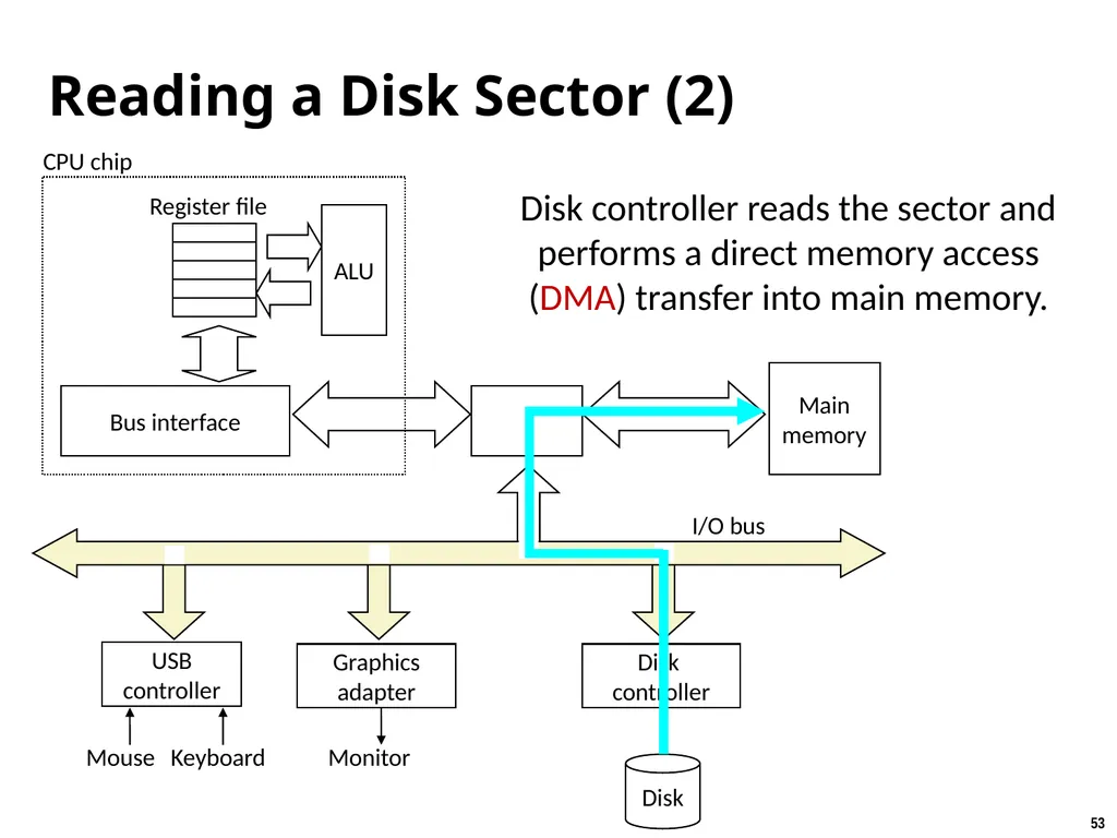
Reading a Disk Sector (2) Register file CPU chip Mouse Keyboard Monitor I/O bus Disk controller reads the sector and performs a direct memory access (DMA) transfer into main memory.<br>
54
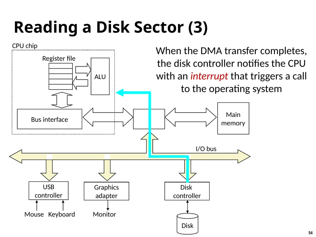
Reading a Disk Sector (3) Register file CPU chip Mouse Keyboard Monitor I/O bus When the DMA transfer completes, the disk controller notifies the CPU with an interrupt that triggers a call to the operating system<br>
55
Nonvolatile Memories DRAM and SRAM are volatile memories
Lose information if powered off.
Nonvolatile memories retain value even if powered off
Read-only memory (ROM): programmed during production
Electrically erasable PROM (EEPROM): electronic erase capability
Flash memory: EEPROMs, with partial (block-level) erase capability
Wears out after 1,000 to 100,000 erasures
Emerging NVMs: MRAM, ReRAM, phase-change memory
Intel’s 3D XPoint (Optane) was discontinued in 2022
Uses for Nonvolatile Memories
Firmware programs stored in a ROM (BIOS, controllers for disks, network cards, graphics accelerators, security subsystems,…)
Solid state disks (replacing rotating disks)
Disk caches<br>
Lose information if powered off.
Nonvolatile memories retain value even if powered off
Read-only memory (ROM): programmed during production
Electrically erasable PROM (EEPROM): electronic erase capability
Flash memory: EEPROMs, with partial (block-level) erase capability
Wears out after 1,000 to 100,000 erasures
Emerging NVMs: MRAM, ReRAM, phase-change memory
Intel’s 3D XPoint (Optane) was discontinued in 2022
Uses for Nonvolatile Memories
Firmware programs stored in a ROM (BIOS, controllers for disks, network cards, graphics accelerators, security subsystems,…)
Solid state disks (replacing rotating disks)
Disk caches<br>
56
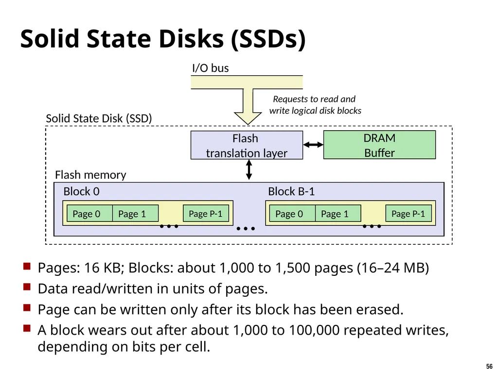
Solid State Disks (SSDs) Pages: 16 KB; Blocks: about 1,000 to 1,500 pages (16–24 MB)
Data read/written in units of pages.
Page can be written only after its block has been erased.
A block wears out after about 1,000 to 100,000 repeated writes, depending on bits per cell. I/O bus … Block 0 … … Block B-1 Flash memory Solid State Disk (SSD) Requests to read and
write logical disk blocks<br>
Data read/written in units of pages.
Page can be written only after its block has been erased.
A block wears out after about 1,000 to 100,000 repeated writes, depending on bits per cell. I/O bus … Block 0 … … Block B-1 Flash memory Solid State Disk (SSD) Requests to read and
write logical disk blocks<br>
57
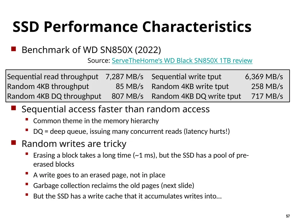
SSD Performance Characteristics Benchmark of WD SN850X (2022)
Sequential access faster than random access
Common theme in the memory hierarchy
DQ = deep queue, issuing many concurrent reads (latency hurts!)
Random writes are tricky
Erasing a block takes a long time (~1 ms), but the SSD has a pool of pre-erased blocks
A write goes to an erased page, not in place
Garbage collection reclaims the old pages (next slide)
But the SSD has a write cache that it accumulates writes into… Sequential read throughput 7,287 MB/s Sequential write tput 6,369 MB/s
Random 4KB throughput 85 MB/s Random 4KB write tput 258 MB/s
Random 4KB DQ throughput 807 MB/s Random 4KB DQ write tput 717 MB/s Source: ServeTheHome’s WD Black SN850X 1TB review<br>
Sequential access faster than random access
Common theme in the memory hierarchy
DQ = deep queue, issuing many concurrent reads (latency hurts!)
Random writes are tricky
Erasing a block takes a long time (~1 ms), but the SSD has a pool of pre-erased blocks
A write goes to an erased page, not in place
Garbage collection reclaims the old pages (next slide)
But the SSD has a write cache that it accumulates writes into… Sequential read throughput 7,287 MB/s Sequential write tput 6,369 MB/s
Random 4KB throughput 85 MB/s Random 4KB write tput 258 MB/s
Random 4KB DQ throughput 807 MB/s Random 4KB DQ write tput 717 MB/s Source: ServeTheHome’s WD Black SN850X 1TB review<br>
58
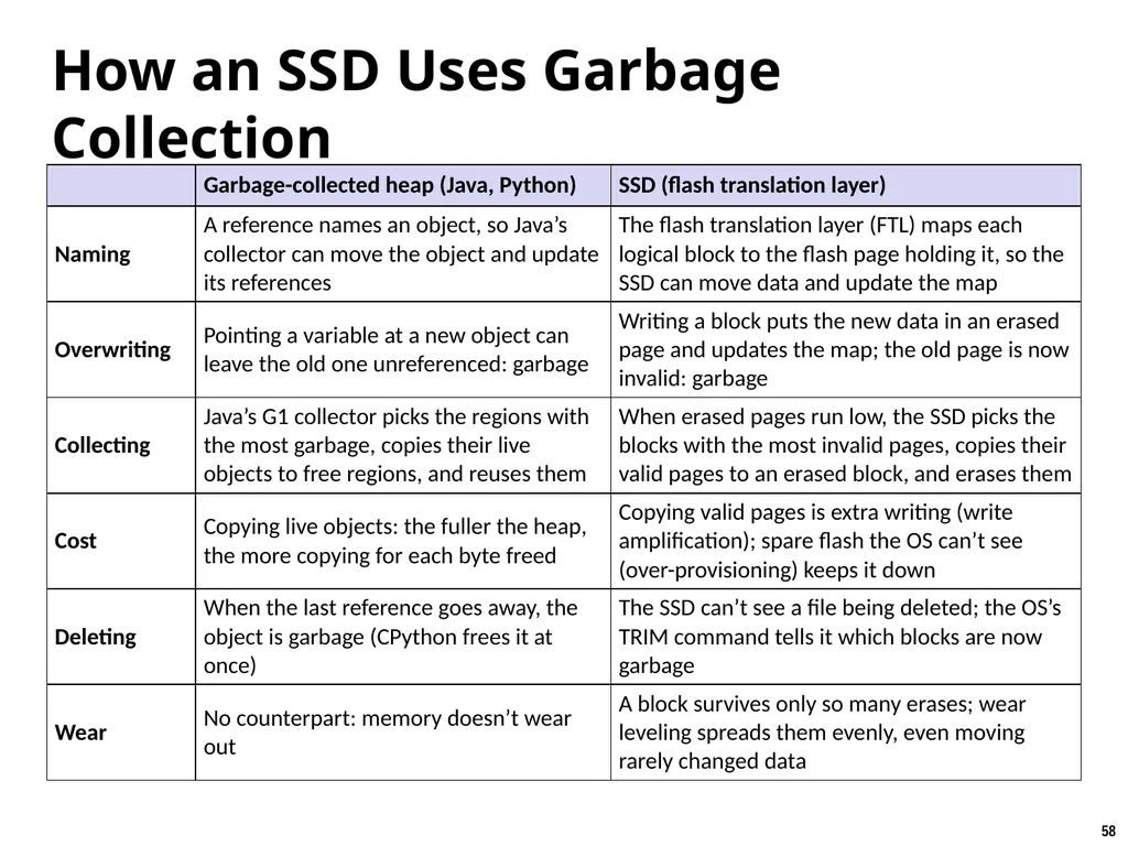
How an SSD Uses Garbage Collection<br>
59
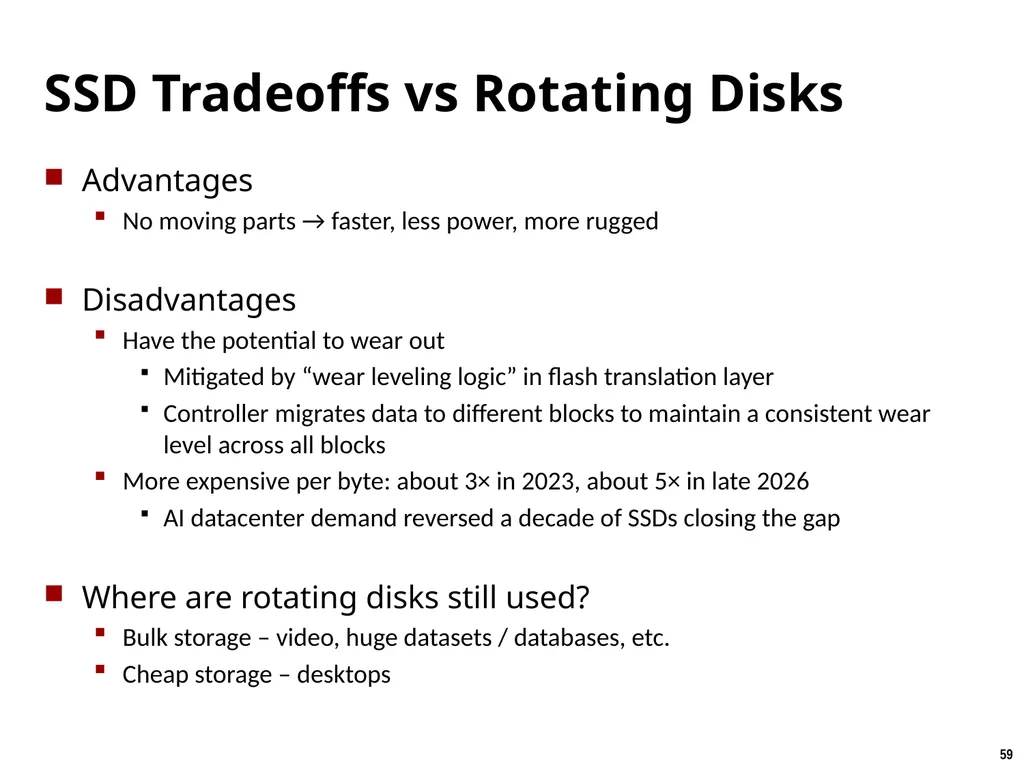
SSD Tradeoffs vs Rotating Disks Advantages
No moving parts → faster, less power, more rugged
Disadvantages
Have the potential to wear out
Mitigated by “wear leveling logic” in flash translation layer
Controller migrates data to different blocks to maintain a consistent wear level across all blocks
More expensive per byte: about 3× in 2023, about 5× in late 2026
AI datacenter demand reversed a decade of SSDs closing the gap
Where are rotating disks still used?
Bulk storage – video, huge datasets / databases, etc.
Cheap storage – desktops<br>
No moving parts → faster, less power, more rugged
Disadvantages
Have the potential to wear out
Mitigated by “wear leveling logic” in flash translation layer
Controller migrates data to different blocks to maintain a consistent wear level across all blocks
More expensive per byte: about 3× in 2023, about 5× in late 2026
AI datacenter demand reversed a decade of SSDs closing the gap
Where are rotating disks still used?
Bulk storage – video, huge datasets / databases, etc.
Cheap storage – desktops<br>
60
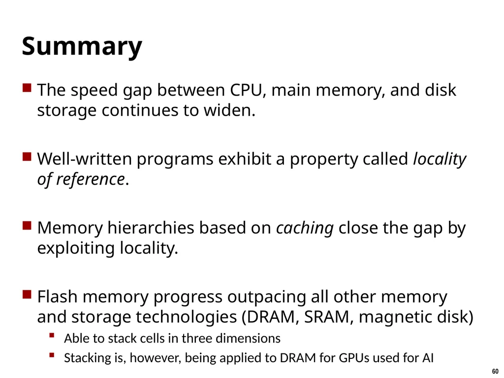
Summary The speed gap between CPU, main memory, and disk storage continues to widen.
Well-written programs exhibit a property called locality of reference.
Memory hierarchies based on caching close the gap by exploiting locality.
Flash memory progress outpacing all other memory and storage technologies (DRAM, SRAM, magnetic disk)
Able to stack cells in three dimensions
Stacking is, however, being applied to DRAM for GPUs used for AI<br>
Well-written programs exhibit a property called locality of reference.
Memory hierarchies based on caching close the gap by exploiting locality.
Flash memory progress outpacing all other memory and storage technologies (DRAM, SRAM, magnetic disk)
Able to stack cells in three dimensions
Stacking is, however, being applied to DRAM for GPUs used for AI<br>
61
Instructor:
Alan L. Cox Cache Memories COMP 222: Introduction to Computer Organization Many slides adapted from Bryant and O’Hallaron, Computer Systems: A Programmer’s Perspective, Third Edition<br>
Alan L. Cox Cache Memories COMP 222: Introduction to Computer Organization Many slides adapted from Bryant and O’Hallaron, Computer Systems: A Programmer’s Perspective, Third Edition<br>
62
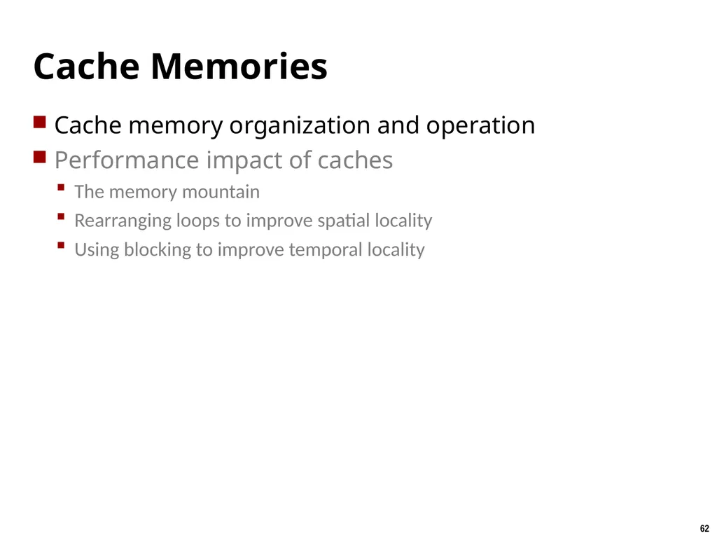
Cache Memories Cache memory organization and operation
Performance impact of caches
The memory mountain
Rearranging loops to improve spatial locality
Using blocking to improve temporal locality<br>
Performance impact of caches
The memory mountain
Rearranging loops to improve spatial locality
Using blocking to improve temporal locality<br>
63
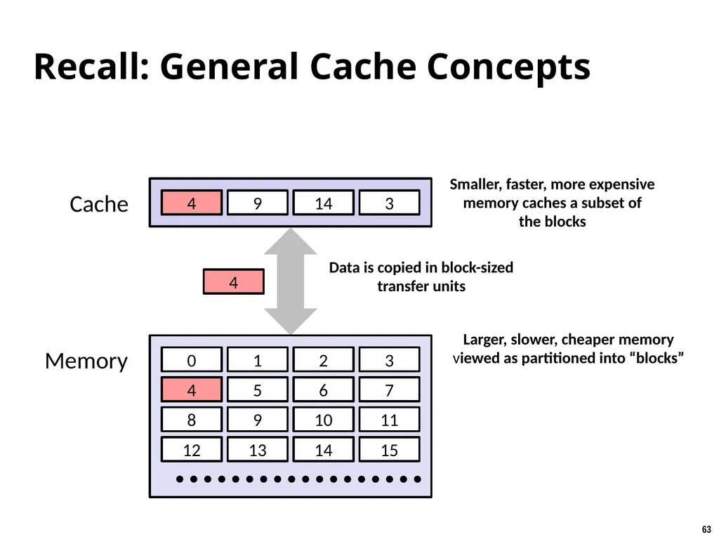
Recall: General Cache Concepts 0 1 2 3 4 5 6 7 8 9 10 11 12 13 14 15 8 9 14 3 Cache Memory Larger, slower, cheaper memory
viewed as partitioned into “blocks” Data is copied in block-sized transfer units Smaller, faster, more expensive
memory caches a subset of
the blocks 4 4 4<br>
viewed as partitioned into “blocks” Data is copied in block-sized transfer units Smaller, faster, more expensive
memory caches a subset of
the blocks 4 4 4<br>
64
General Cache Concepts: Hit 0 1 2 3 4 5 6 7 8 9 10 11 12 13 14 15 8 9 14 3 Cache Memory Data in block b is needed Request: 14 14 Block b is in cache:
Hit!<br>
Hit!<br>
65
General Cache Concepts: Miss 0 1 2 3 4 5 6 7 8 9 10 11 12 13 14 15 8 9 14 3 Cache Memory Data in block b is needed Request: 12 Block b is not in cache:
Miss! Block b is fetched from
memory Request: 12 12 12 12 Block b is stored in cache
Placement policy: determines where b goes
Replacement policy: determines which block gets evicted (victim)<br>
Miss! Block b is fetched from
memory Request: 12 12 12 12 Block b is stored in cache
Placement policy: determines where b goes
Replacement policy: determines which block gets evicted (victim)<br>
66
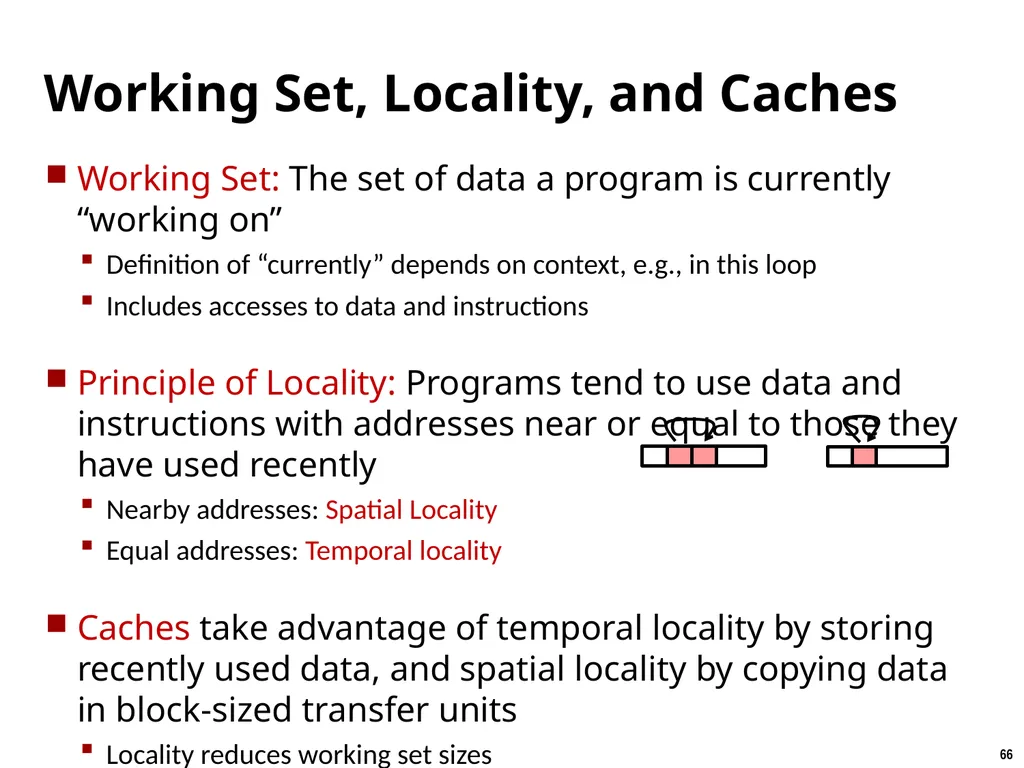
Working Set, Locality, and Caches Working Set: The set of data a program is currently “working on”
Definition of “currently” depends on context, e.g., in this loop
Includes accesses to data and instructions
Principle of Locality: Programs tend to use data and instructions with addresses near or equal to those they have used recently
Nearby addresses: Spatial Locality
Equal addresses: Temporal locality
Caches take advantage of temporal locality by storing recently used data, and spatial locality by copying data in block-sized transfer units
Locality reduces working set sizes
Caches are most effective when the working set fits in the cache<br>
Definition of “currently” depends on context, e.g., in this loop
Includes accesses to data and instructions
Principle of Locality: Programs tend to use data and instructions with addresses near or equal to those they have used recently
Nearby addresses: Spatial Locality
Equal addresses: Temporal locality
Caches take advantage of temporal locality by storing recently used data, and spatial locality by copying data in block-sized transfer units
Locality reduces working set sizes
Caches are most effective when the working set fits in the cache<br>
67
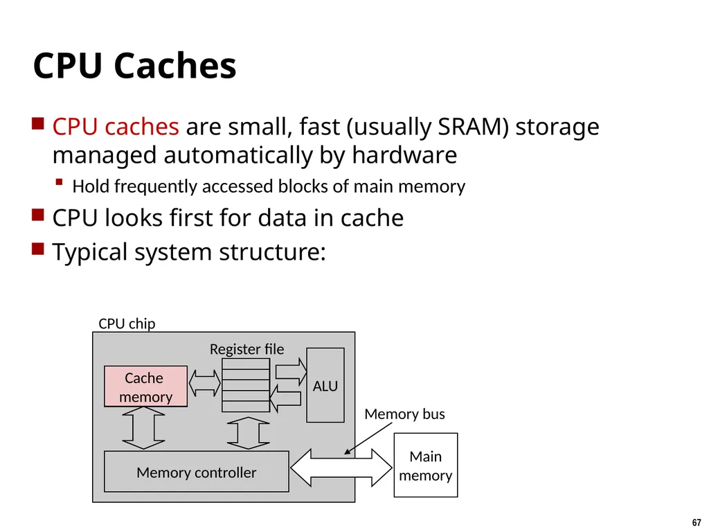
CPU Caches CPU caches are small, fast (usually SRAM) storage managed automatically by hardware
Hold frequently accessed blocks of main memory
CPU looks first for data in cache
Typical system structure: Main
memory Memory controller ALU Register file CPU chip Memory bus Cache
memory<br>
Hold frequently accessed blocks of main memory
CPU looks first for data in cache
Typical system structure: Main
memory Memory controller ALU Register file CPU chip Memory bus Cache
memory<br>
68
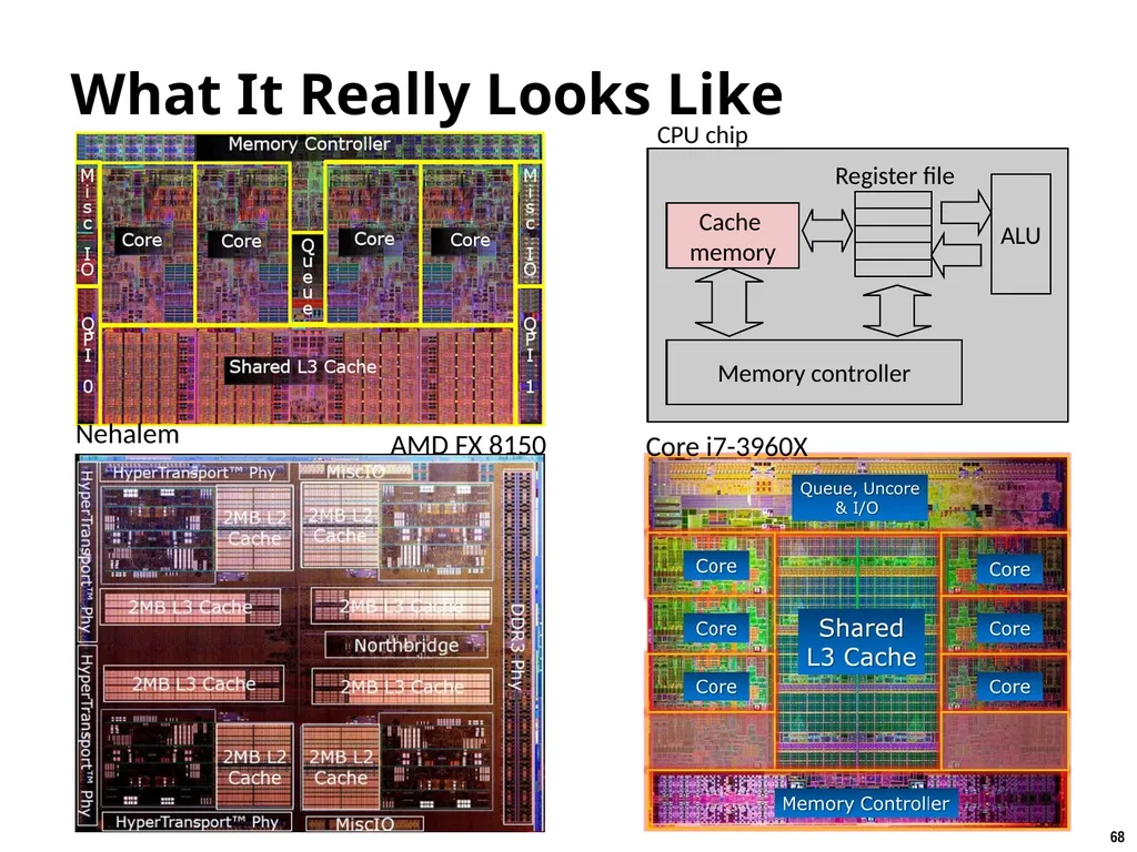
What It Really Looks Like Memory controller ALU Register file CPU chip Cache
memory Core i7-3960X AMD FX 8150 Nehalem<br>
memory Core i7-3960X AMD FX 8150 Nehalem<br>
69
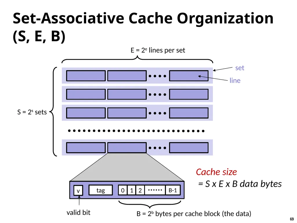
Set-Associative Cache Organization (S, E, B) E = 2e lines per set S = 2s sets set line 0 1 2 B-1 tag v B = 2b bytes per cache block (the data) Cache size
= S x E x B data bytes valid bit<br>
= S x E x B data bytes valid bit<br>
70
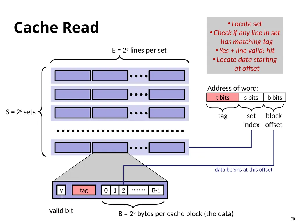
Cache Read E = 2e lines per set S = 2s sets 0 1 2 B-1 tag v valid bit B = 2b bytes per cache block (the data) t bits s bits b bits Address of word: tag set
index block
offset data begins at this offset Locate set
Check if any line in set has matching tag
Yes + line valid: hit
Locate data starting at offset<br>
index block
offset data begins at this offset Locate set
Check if any line in set has matching tag
Yes + line valid: hit
Locate data starting at offset<br>
71
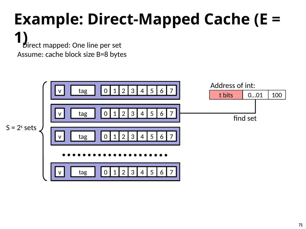
Example: Direct-Mapped Cache (E = 1) S = 2s sets Direct mapped: One line per set
Assume: cache block size B=8 bytes t bits 0…01 100 Address of int: 0 1 2 7 tag v 3 6 5 4 0 1 2 7 tag v 3 6 5 4 0 1 2 7 tag v 3 6 5 4 0 1 2 7 tag v 3 6 5 4 find set<br>
Assume: cache block size B=8 bytes t bits 0…01 100 Address of int: 0 1 2 7 tag v 3 6 5 4 0 1 2 7 tag v 3 6 5 4 0 1 2 7 tag v 3 6 5 4 0 1 2 7 tag v 3 6 5 4 find set<br>
72
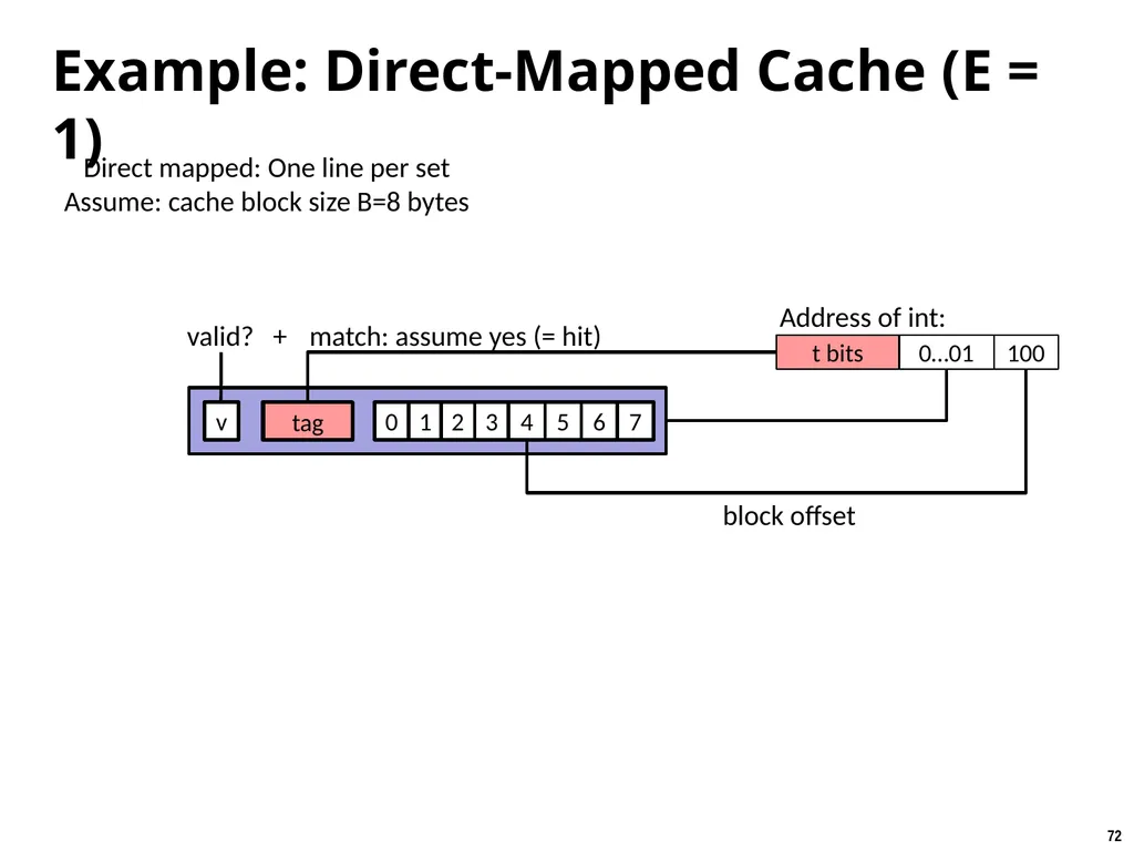
Example: Direct-Mapped Cache (E = 1) Direct mapped: One line per set
Assume: cache block size B=8 bytes t bits 0…01 100 Address of int: 0 1 2 7 tag v 3 6 5 4 match: assume yes (= hit) valid? + block offset tag<br>
Assume: cache block size B=8 bytes t bits 0…01 100 Address of int: 0 1 2 7 tag v 3 6 5 4 match: assume yes (= hit) valid? + block offset tag<br>
73
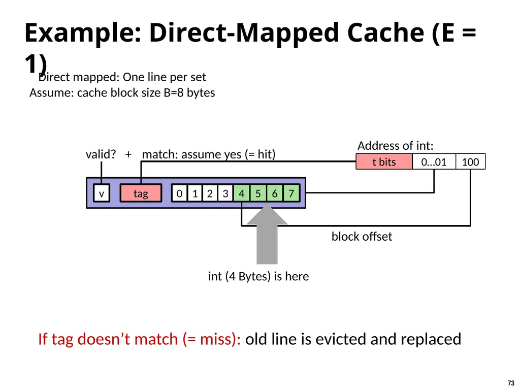
Example: Direct-Mapped Cache (E = 1) Direct mapped: One line per set
Assume: cache block size B=8 bytes t bits 0…01 100 Address of int: 0 1 2 7 tag v 3 6 5 4 match: assume yes (= hit) valid? + int (4 Bytes) is here block offset If tag doesn’t match (= miss): old line is evicted and replaced<br>
Assume: cache block size B=8 bytes t bits 0…01 100 Address of int: 0 1 2 7 tag v 3 6 5 4 match: assume yes (= hit) valid? + int (4 Bytes) is here block offset If tag doesn’t match (= miss): old line is evicted and replaced<br>
74
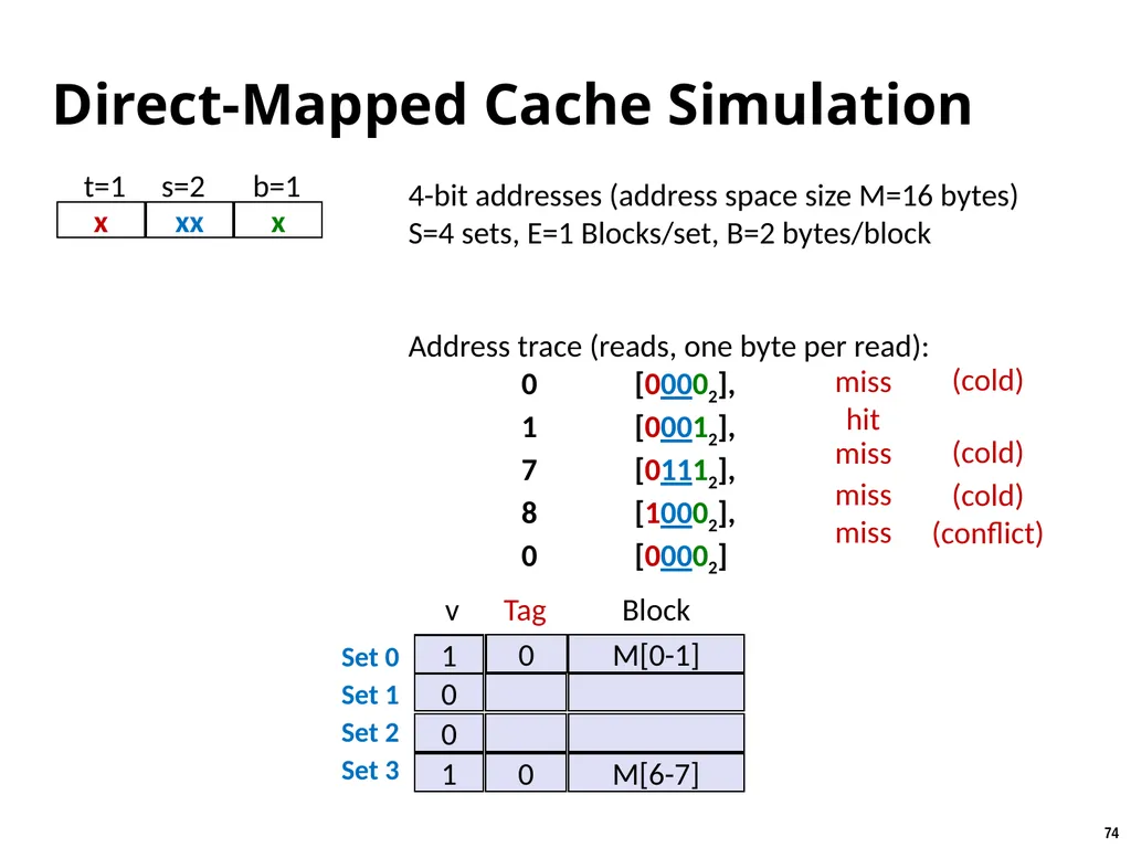
Direct-Mapped Cache Simulation 4-bit addresses (address space size M=16 bytes)
S=4 sets, E=1 Blocks/set, B=2 bytes/block
Address trace (reads, one byte per read):
0 [00002],
1 [00012],
7 [01112],
8 [10002],
0 [00002] x t=1 s=2 b=1 xx x v Tag Block 0 0 0 miss hit miss miss miss Set 0 Set 1 Set 2 Set 3 (cold) (cold) (cold) (conflict)<br>
S=4 sets, E=1 Blocks/set, B=2 bytes/block
Address trace (reads, one byte per read):
0 [00002],
1 [00012],
7 [01112],
8 [10002],
0 [00002] x t=1 s=2 b=1 xx x v Tag Block 0 0 0 miss hit miss miss miss Set 0 Set 1 Set 2 Set 3 (cold) (cold) (cold) (conflict)<br>
75
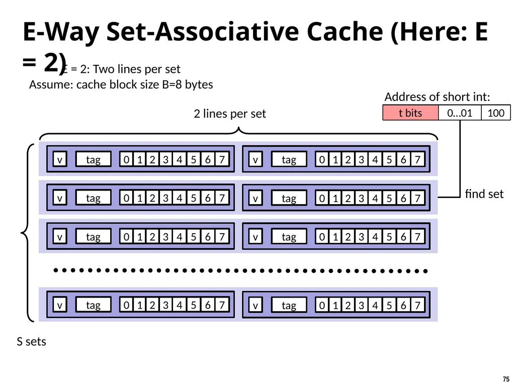
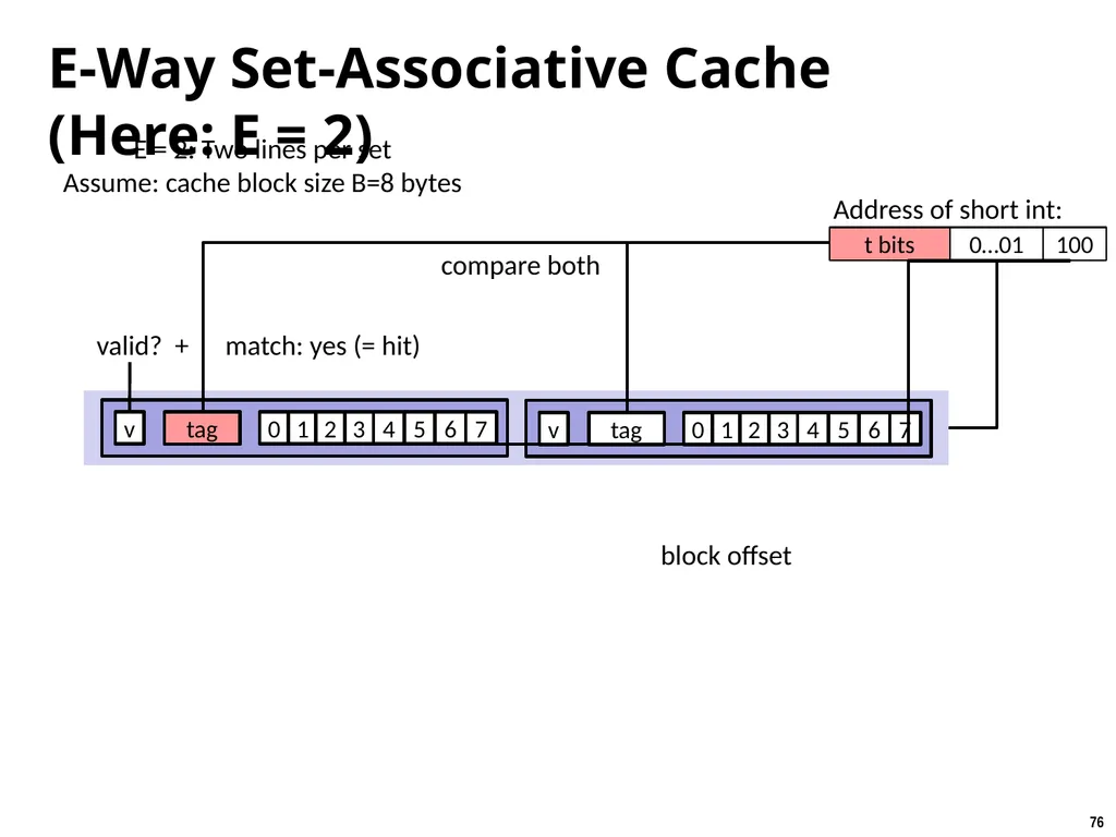
E-Way Set-Associative Cache (Here: E = 2) E = 2: Two lines per set
Assume: cache block size B=8 bytes t bits 0…01 100 Address of short int: 0 1 2 7 tag v 3 6 5 4 0 1 2 7 tag v 3 6 5 4 0 1 2 7 tag v 3 6 5 4 0 1 2 7 tag v 3 6 5 4 0 1 2 7 tag v 3 6 5 4 0 1 2 7 tag v 3 6 5 4 0 1 2 7 tag v 3 6 5 4 0 1 2 7 tag v 3 6 5 4 find set 2 lines per set S sets<br>
Assume: cache block size B=8 bytes t bits 0…01 100 Address of short int: 0 1 2 7 tag v 3 6 5 4 0 1 2 7 tag v 3 6 5 4 0 1 2 7 tag v 3 6 5 4 0 1 2 7 tag v 3 6 5 4 0 1 2 7 tag v 3 6 5 4 0 1 2 7 tag v 3 6 5 4 0 1 2 7 tag v 3 6 5 4 0 1 2 7 tag v 3 6 5 4 find set 2 lines per set S sets<br>
76
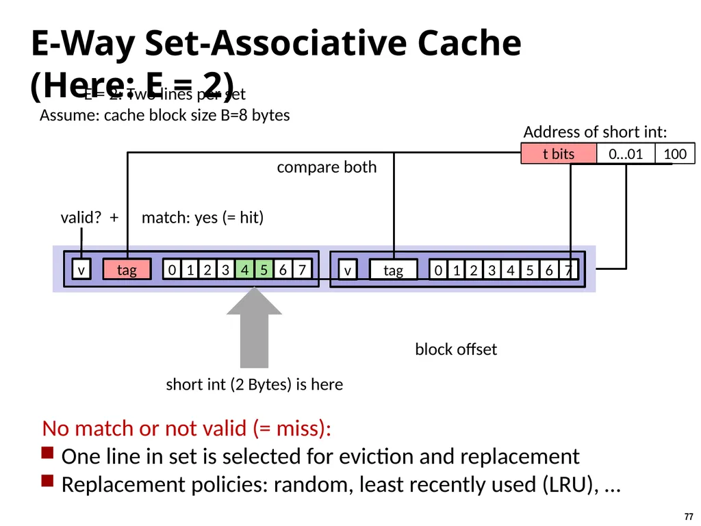
E-Way Set-Associative Cache (Here: E = 2) E = 2: Two lines per set
Assume: cache block size B=8 bytes t bits 0…01 100 Address of short int: 0 1 2 7 tag v 3 6 5 4 0 1 2 7 tag v 3 6 5 4 compare both valid? + match: yes (= hit) block offset tag<br>
Assume: cache block size B=8 bytes t bits 0…01 100 Address of short int: 0 1 2 7 tag v 3 6 5 4 0 1 2 7 tag v 3 6 5 4 compare both valid? + match: yes (= hit) block offset tag<br>
77
E-Way Set-Associative Cache (Here: E = 2) E = 2: Two lines per set
Assume: cache block size B=8 bytes t bits 0…01 100 Address of short int: 0 1 2 7 tag v 3 6 5 4 0 1 2 7 tag v 3 6 5 4 compare both valid? + match: yes (= hit) block offset tag 5 4 short int (2 Bytes) is here No match or not valid (= miss):
One line in set is selected for eviction and replacement
Replacement policies: random, least recently used (LRU), …<br>
Assume: cache block size B=8 bytes t bits 0…01 100 Address of short int: 0 1 2 7 tag v 3 6 5 4 0 1 2 7 tag v 3 6 5 4 compare both valid? + match: yes (= hit) block offset tag 5 4 short int (2 Bytes) is here No match or not valid (= miss):
One line in set is selected for eviction and replacement
Replacement policies: random, least recently used (LRU), …<br>
78
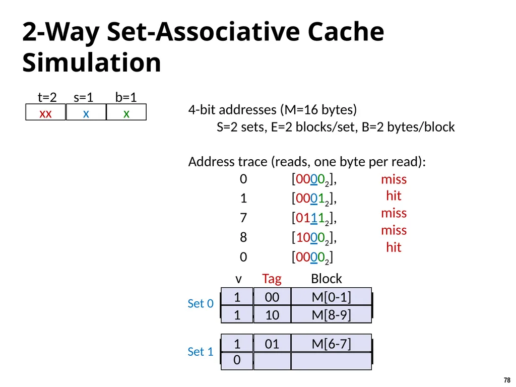
2-Way Set-Associative Cache Simulation 4-bit addresses (M=16 bytes)
S=2 sets, E=2 blocks/set, B=2 bytes/block
Address trace (reads, one byte per read):
0 [00002],
1 [00012],
7 [01112],
8 [10002],
0 [00002] xx t=2 s=1 b=1 x x v Tag Block 0 0 0 miss hit miss miss hit Set 0 Set 1<br>
S=2 sets, E=2 blocks/set, B=2 bytes/block
Address trace (reads, one byte per read):
0 [00002],
1 [00012],
7 [01112],
8 [10002],
0 [00002] xx t=2 s=1 b=1 x x v Tag Block 0 0 0 miss hit miss miss hit Set 0 Set 1<br>
79
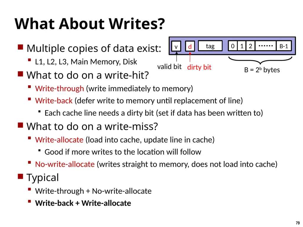
What About Writes? Multiple copies of data exist:
L1, L2, L3, Main Memory, Disk
What to do on a write-hit?
Write-through (write immediately to memory)
Write-back (defer write to memory until replacement of line)
Each cache line needs a dirty bit (set if data has been written to)
What to do on a write-miss?
Write-allocate (load into cache, update line in cache)
Good if more writes to the location will follow
No-write-allocate (writes straight to memory, does not load into cache)
Typical
Write-through + No-write-allocate
Write-back + Write-allocate<br>
L1, L2, L3, Main Memory, Disk
What to do on a write-hit?
Write-through (write immediately to memory)
Write-back (defer write to memory until replacement of line)
Each cache line needs a dirty bit (set if data has been written to)
What to do on a write-miss?
Write-allocate (load into cache, update line in cache)
Good if more writes to the location will follow
No-write-allocate (writes straight to memory, does not load into cache)
Typical
Write-through + No-write-allocate
Write-back + Write-allocate<br>
80
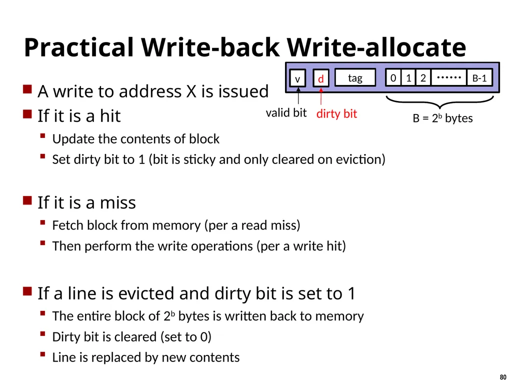
Practical Write-back Write-allocate A write to address X is issued
If it is a hit
Update the contents of block
Set dirty bit to 1 (bit is sticky and only cleared on eviction)
If it is a miss
Fetch block from memory (per a read miss)
Then perform the write operations (per a write hit)
If a line is evicted and dirty bit is set to 1
The entire block of 2b bytes is written back to memory
Dirty bit is cleared (set to 0)
Line is replaced by new contents<br>
If it is a hit
Update the contents of block
Set dirty bit to 1 (bit is sticky and only cleared on eviction)
If it is a miss
Fetch block from memory (per a read miss)
Then perform the write operations (per a write hit)
If a line is evicted and dirty bit is set to 1
The entire block of 2b bytes is written back to memory
Dirty bit is cleared (set to 0)
Line is replaced by new contents<br>
81
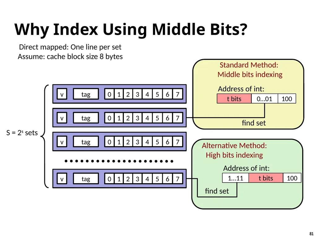
Why Index Using Middle Bits? S = 2s sets Direct mapped: One line per set
Assume: cache block size 8 bytes 0 1 2 7 tag v 3 6 5 4 0 1 2 7 tag v 3 6 5 4 0 1 2 7 tag v 3 6 5 4 0 1 2 7 tag v 3 6 5 4<br>
Assume: cache block size 8 bytes 0 1 2 7 tag v 3 6 5 4 0 1 2 7 tag v 3 6 5 4 0 1 2 7 tag v 3 6 5 4 0 1 2 7 tag v 3 6 5 4<br>
82
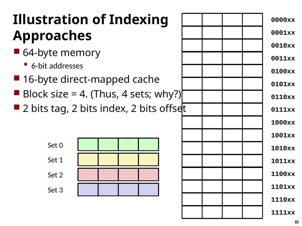
Illustration of Indexing Approaches 64-byte memory
6-bit addresses
16-byte direct-mapped cache
Block size = 4. (Thus, 4 sets; why?)
2 bits tag, 2 bits index, 2 bits offset Set 0 Set 1 Set 2 Set 3 1111xx 1110xx 1101xx 1100xx 1011xx 1010xx 1001xx 1000xx 0111xx 0110xx 0101xx 0100xx 0011xx 0010xx 0001xx 0000xx<br>
6-bit addresses
16-byte direct-mapped cache
Block size = 4. (Thus, 4 sets; why?)
2 bits tag, 2 bits index, 2 bits offset Set 0 Set 1 Set 2 Set 3 1111xx 1110xx 1101xx 1100xx 1011xx 1010xx 1001xx 1000xx 0111xx 0110xx 0101xx 0100xx 0011xx 0010xx 0001xx 0000xx<br>
83
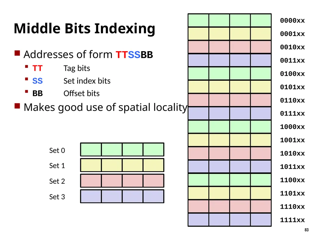
Middle Bits Indexing Addresses of form TTSSBB
TT Tag bits
SS Set index bits
BB Offset bits
Makes good use of spatial locality Set 0 Set 1 Set 2 Set 3 1111xx 1110xx 1101xx 1100xx 1011xx 1010xx 1001xx 1000xx 0111xx 0110xx 0101xx 0100xx 0011xx 0010xx 0001xx 0000xx<br>
TT Tag bits
SS Set index bits
BB Offset bits
Makes good use of spatial locality Set 0 Set 1 Set 2 Set 3 1111xx 1110xx 1101xx 1100xx 1011xx 1010xx 1001xx 1000xx 0111xx 0110xx 0101xx 0100xx 0011xx 0010xx 0001xx 0000xx<br>
84
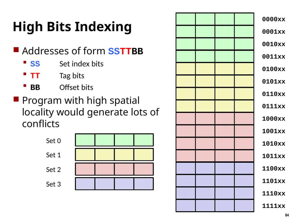
High Bits Indexing Addresses of form SSTTBB
SS Set index bits
TT Tag bits
BB Offset bits
Program with high spatial locality would generate lots of conflicts Set 0 Set 1 Set 2 Set 3 1111xx 1110xx 1101xx 1100xx 1011xx 1010xx 1001xx 1000xx 0111xx 0110xx 0101xx 0100xx 0011xx 0010xx 0001xx 0000xx<br>
SS Set index bits
TT Tag bits
BB Offset bits
Program with high spatial locality would generate lots of conflicts Set 0 Set 1 Set 2 Set 3 1111xx 1110xx 1101xx 1100xx 1011xx 1010xx 1001xx 1000xx 0111xx 0110xx 0101xx 0100xx 0011xx 0010xx 0001xx 0000xx<br>
85
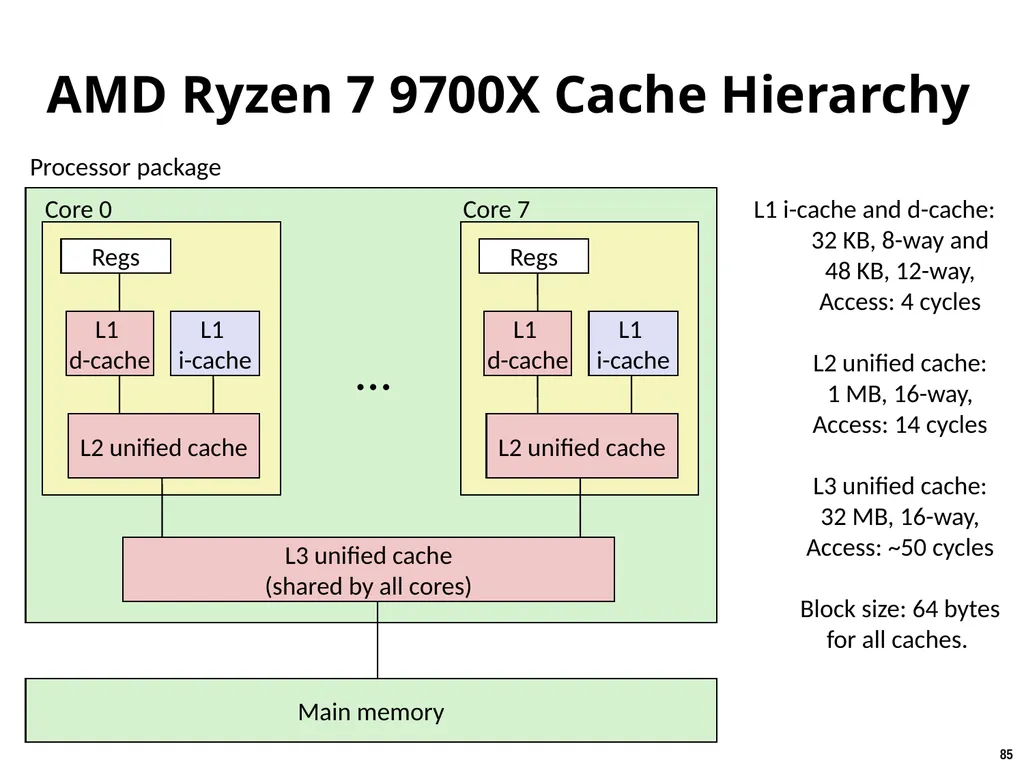
AMD Ryzen 7 9700X Cache Hierarchy Regs L1
d-cache L1
i-cache L2 unified cache Core 0 Regs L1
d-cache L1
i-cache L2 unified cache Core 7 … L3 unified cache
(shared by all cores) Main memory Processor package L1 i-cache and d-cache:
32 KB, 8-way and
48 KB, 12-way,
Access: 4 cycles
L2 unified cache:
1 MB, 16-way,
Access: 14 cycles
L3 unified cache:
32 MB, 16-way,
Access: ~50 cycles
Block size: 64 bytes for all caches.<br>
d-cache L1
i-cache L2 unified cache Core 0 Regs L1
d-cache L1
i-cache L2 unified cache Core 7 … L3 unified cache
(shared by all cores) Main memory Processor package L1 i-cache and d-cache:
32 KB, 8-way and
48 KB, 12-way,
Access: 4 cycles
L2 unified cache:
1 MB, 16-way,
Access: 14 cycles
L3 unified cache:
32 MB, 16-way,
Access: ~50 cycles
Block size: 64 bytes for all caches.<br>
86
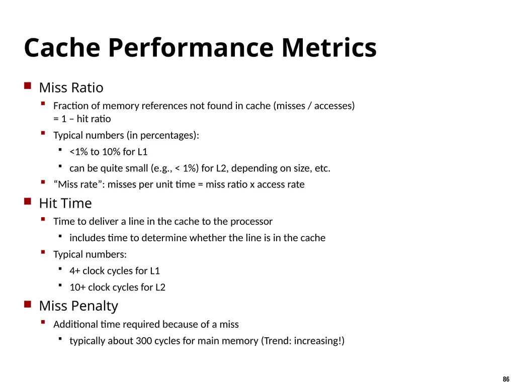
Cache Performance Metrics Miss Ratio
Fraction of memory references not found in cache (misses / accesses) = 1 – hit ratio
Typical numbers (in percentages):
<1% to 10% for L1
can be quite small (e.g., < 1%) for L2, depending on size, etc.
“Miss rate”: misses per unit time = miss ratio x access rate
Hit Time
Time to deliver a line in the cache to the processor
includes time to determine whether the line is in the cache
Typical numbers:
4+ clock cycles for L1
10+ clock cycles for L2
Miss Penalty
Additional time required because of a miss
typically about 300 cycles for main memory (Trend: increasing!)<br>
Fraction of memory references not found in cache (misses / accesses) = 1 – hit ratio
Typical numbers (in percentages):
<1% to 10% for L1
can be quite small (e.g., < 1%) for L2, depending on size, etc.
“Miss rate”: misses per unit time = miss ratio x access rate
Hit Time
Time to deliver a line in the cache to the processor
includes time to determine whether the line is in the cache
Typical numbers:
4+ clock cycles for L1
10+ clock cycles for L2
Miss Penalty
Additional time required because of a miss
typically about 300 cycles for main memory (Trend: increasing!)<br>
87
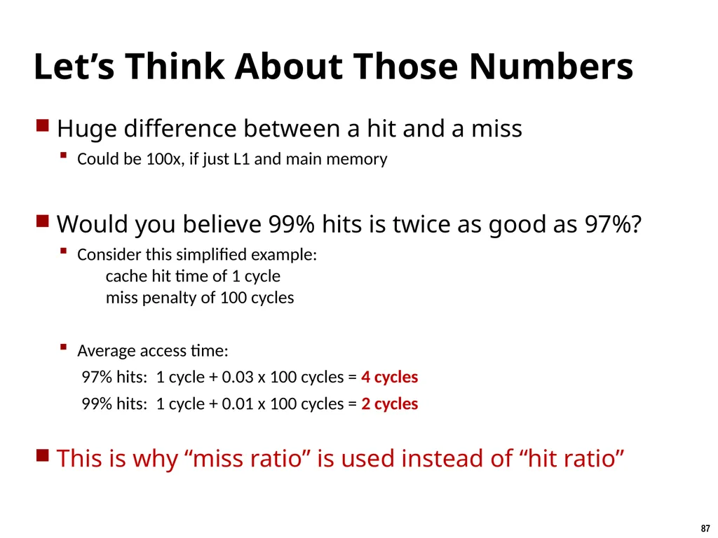
Let’s Think About Those Numbers Huge difference between a hit and a miss
Could be 100x, if just L1 and main memory
Would you believe 99% hits is twice as good as 97%?
Consider this simplified example: cache hit time of 1 cycle miss penalty of 100 cycles
Average access time:
97% hits: 1 cycle + 0.03 x 100 cycles = 4 cycles
99% hits: 1 cycle + 0.01 x 100 cycles = 2 cycles
This is why “miss ratio” is used instead of “hit ratio”<br>
Could be 100x, if just L1 and main memory
Would you believe 99% hits is twice as good as 97%?
Consider this simplified example: cache hit time of 1 cycle miss penalty of 100 cycles
Average access time:
97% hits: 1 cycle + 0.03 x 100 cycles = 4 cycles
99% hits: 1 cycle + 0.01 x 100 cycles = 2 cycles
This is why “miss ratio” is used instead of “hit ratio”<br>
88
Writing Cache Friendly Code Make the common case go fast
Focus on the inner loops of the core functions
Minimize the misses in the inner loops
Repeated references to variables are good (temporal locality)
Stride-1 reference patterns are good (spatial locality) Key idea: Our qualitative notion of locality is quantified through our understanding of cache memories<br>
Focus on the inner loops of the core functions
Minimize the misses in the inner loops
Repeated references to variables are good (temporal locality)
Stride-1 reference patterns are good (spatial locality) Key idea: Our qualitative notion of locality is quantified through our understanding of cache memories<br>