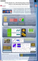
/
Design Studies for a TPC Readout Plane Using Zigzag Patterns with Multistage GEM Detectors Design Studies for a TPC Readout Plane Using Zigzag Patterns with Multistage GEM Detectors

Design Studies for a TPC Readout Plane Using Zigzag Patterns with Multistage GEM Detectors - PowerPoint Presentation

faustina-dinatale
faustina-dinatale . @faustina-dinatale
Follow
370 views
Uploaded On 2019-01-27

Design Studies for a TPC Readout Plane Using Zigzag Patterns with Multistage GEM Detectors - PPT Presentation

B Azmoun 1 P Garg 3 T K Hemmick 3 M Hohlmann 2 A Kiselev 1 M L Purschke 1 C Woody 1 A Zhang 1 1  Brookhaven National Laboratory Physics Department Upton New York United States of America ID: 748490

zigzag pad pads charge pad zigzag charge pads pitch design pcb single sharing resolution gap width performance position hit

Share:

Link:

Embed:

Download Presentation from below link

Download Presentation The PPT/PDF document "Design Studies for a TPC Readout Plane U..." is the property of its rightful owner. Permission is granted to download and print the materials on this web site for personal, non-commercial use only, and to display it on your personal computer provided you do not modify the materials and that you retain all copyright notices contained in the materials. By downloading content from our website, you accept the terms of this agreement.


Presentation Transcript

Slide1

Design Studies for a TPC Readout Plane Using Zigzag Patterns with Multistage GEM DetectorsB. Azmoun1, P. Garg3, T. K. Hemmick3, M. Hohlmann2, A. Kiselev1, M. L. Purschke1, C. Woody1, A. Zhang11 Brookhaven National Laboratory, Physics Department, Upton, New York, United States of America2 Florida Institute of Technology, Department of Physics & Space Sciences, Melbourne, Florida, United States of America3Stony Brook University, Department of Physics and Astronomy, Stony Brook, New York, United States of America

INTRODUCTION

A

Time Projection Chamber (TPC) is currently under development for the

sPHENIX detector at RHIC. It

will be read out using a multi-stage GEM detector at each endcap, with a pad-plane consisting of 40 pad rows in radius. A critical performance goal for the readout is to achieve a minimal single point spatial resolution of ~200mm. In order to meet this requirement with minimal channel count and cost, we propose segmenting the readout into zigzag-shaped pads with a pitch of about 2mm and a length of about 1cm. The interleaving tips of the zigzags enhance .

sharing between neighboring pads and allow the possibility to interpolate the hit position to a precision many times better than the physical extent of the pad itself. Here we discuss various simulation studies that were employed to optimize the size and shape of the zigzag pattern, along with the challenges in fabricating the corresponding PCB’s. Finally, results will be presented of a prototype zigzag PCB studied in the lab.

SUMMARY AND CONCLUSIONS

In large part, these results were able to validate the fundamental concepts behind the charge sharing model described above. This is seen by the improved performance of the newer board compared to the older one. However, the new board is still far from ideal. In fact the fabrication process imposes some real constraints on the deliverable geometric parameters of the zigzag pattern. For the new PCB, the larger feature sizes, including the zigzag pitch and period were reproduced quite accurately by the manufacturer, however the smaller features like the trace and gap width had a margin of error approaching 5-10%. In particular, the zigzag geometry was distorted by both the over-etching of the zigzag tips and the trace width and by under-etching the zigzag troughs. The over-etched tips resulted in reducing the pad overlap from 94% in the design to 82% for the fabricated PCB. In addition, the area occupied by the copper conductor was diminished from 67% to 63%. We plan to continue the development and optimization of the zigzag pads, with a focus on pursuing

more accurate fabrication methods. In particular, a laser etching process is available at reasonable cost, which seems to be among the most accurate fabrication techniques available on the market. Feature sizes down to about 25mm (~1mil) are possible with this technique, far out-performing the specifications of traditional chemical etching. Thus we plan to have new PCB’s made using this process which provides smaller gaps between zigzag pads and increased pad overlap, for potentially improved performance.

Motivation: Linear Charge Sharing Model

Zigzag overlap

Pad

width

No

overlap

Tip-

toTip

Distance

Hit position of charge cloud

(Assuming no single pad hits, which

is an ideal feature of zigzags)


(For single pad hits)


6 Zigzag pads, 2mm

pitch

6 Rect. pads, 2mm

pitch

Attributes:

Charge sharing is directly proportional to hit position as long as the pitch and period are chosen appropriately for the

size of the charge cloud

T

he pad response is independent

o

f charge cloud size over a relatively broad range of sizes

2-3 pads are needed for the centroid calculation; additional pads tend to deteriorate linearity

Ideally, a

single strip does not take more than ~80% of total charge

Ideally, the pad

response is independent of hit

position, with a differential non-linearity (

DNL)

~ 0

Single pad hits

should be

minimized

to ~

0

In principle there are no limiting factors for the achievable position resolution

due to the use of

ideal ZZ pads,

other than

practical issues like signal to noise ratio,

etc

An optimized pad design avoids

corrections for

a DNL, which are never 100% efficient

The ideal geometry of zigzags offer a scheme to split charge in proportion to hit position, while allowing the pad to extend well beyond the pitch – typically the pad extends two times the pitch.

Generally, the pitch and the

degree of interleaving of the zigzag tips determine the level of charge sharing uniformity, where the zigzag period can influence the “flatness of responseAs can be seen below, the more practical parameters like trace and gap width play a significant role with regard to the actual achievable resolution

Simulations

Measurements

Scanning

X-ray Gun (Collimated

)

4

-GEM

w/ Zigzag

Readout (ArCO2 (70/30))

Measured physical

ZZ

Parameters

p (mm)

d (mm)

s (mm)g (mm)Strip Overlap / Pitch (%)Gap / Pitch (%)Electrode Area / Tot. PCB Active Area (%)Old Design/PCB2.000.50.1590.08269.04.166.0New Design/PCB2.000.5860.1410.08482.54.263.0

For the same pitch, zigzag shaped pads have clear advantages over standard rectangular pads.

Charge sharing among neighboring pads

Coarse ZigzagNon-uniform response, ie large DNLPoor spatial resolutionSingle pad hits, ie Non-sensitive areas

Highly Interleaved ZigzagUniform response across pad plane,No “dead zones”Very good spatial resolution

Residual Distr.

Residual Vs. hit position

~60mmN/S ~2%

Charge collection simulation, dictated by the simple geometry of the zigzag pattern

An ANSYS simulation of the electric field in the gap above the zigzag pads and a simulation of gas processes like diffusion are used together to track a uniform plane of electrons onto the pad plane

The collection of electrons onto the zigzag pads is done in a quite uniform way, so the electric field does not impose any significant non-uniformity during the collection process

Density of collected electrons

A slit collimated beam of x-rays

(~50

m

m

x 8mm) scans across ZZ readout, coupled to a 4-GEM stackNote: the resolutions quoted here do not have the beam width unfolded, since the width is not precisely known

Biggest improvements in new PCB design include increased interleaving and reduced single pad zone

Old PCB/Design Scan Results

New PCB/Design Scan Results

Performance improvements (New Vs Old PCB):Reduced DNL (more homogeneous response)Improved resolution (70/100mm Vs 98/132mm)Far fewer single pad hits (few% Vs 30%)While the in-lab measurements of resolution may be used to attach figures of merit to each zigzag pattern, these measurements are not fully representative of the single point track resolution in the TPC, therefore the goal is to simply maximize, to a reasonable extent this relative measure of the resolution. In general, the performance is hindered by practical matters like S/N, cross talk, gain uniformity, FEE dynamic range, specific E-field distortions, and fabrication limitations on gap widths, etc.

s ~100mmN/S ~1-3%

s ~70mmN/S ~ 1-3%

Perpendicular Scan

By scanning perpendicularly, the uniformity of the pad response may be checked across the ZZ period

Spectra at all five points have the same shape

 uniform pad response across ZZ periodsSmallest charge for a fired pad is ~10% of total collected charge

Slope ~1

Zigzag Geometry

Critical items:

The over-etched tips may substantially diminish the performance of the PCB (vis-a-vis reduced charge sharing)

Gaps larger than the design spec. and trace widths narrower than the design spec. will also impact the performance by reducing the amount of copper conductor covering the active

area, possibly contributing to non-linear charge sharing

Zigzag Distortions

Zigzags Vs Std. rectangular pads

Charge cloud

Parameter

Definitionp (defining)ZZ pitchd (defining)ZZ periods (defining)Trace widthg (defining)Gap widths’ (secondary)Trace width (apex)g’ (secondary)Gap width (apex)q (secondary)ZZ angle

Ideal pad:

z

ero space-gap

This work was supported by the U.S. Department of Energy under Prime Contract No. DE-ACO2-98CH10886.

Charge ratio spectra at 5 points within a 500mm ZZ period

Min charge

~10%

Centroid Residual (

m

m)

Counts

ZZ period

Collimated x-ray

Line Source

New PCB/Design

Old PCB/Design

Single

Pad Hit

zone

ZZ pitch

ZZ pitch