Explore
Featured
Recent
Articles
Topics
Login
Upload
Featured
Recent
Articles
Topics
Login
Upload
Search Results for 'Lithography-Substrate'
Lithography-Substrate published presentations and documents on DocSlides.
Lithography
by celsa-spraggs
NANO 101. Introduction to Nanotechnology. 1. 2. L...
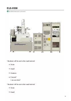
Electron Beam Lithography System HS50
by stselionix
Electron Beam Lithography System HS50
Nanoscale lithography
by liane-varnes
Michael Johnston. 4/13/2015. Abstract and Outline...
LIGA Lithography
by emily
By: Bitew Dinke Hugo Ferrer Enee416 Dr. G hodss...
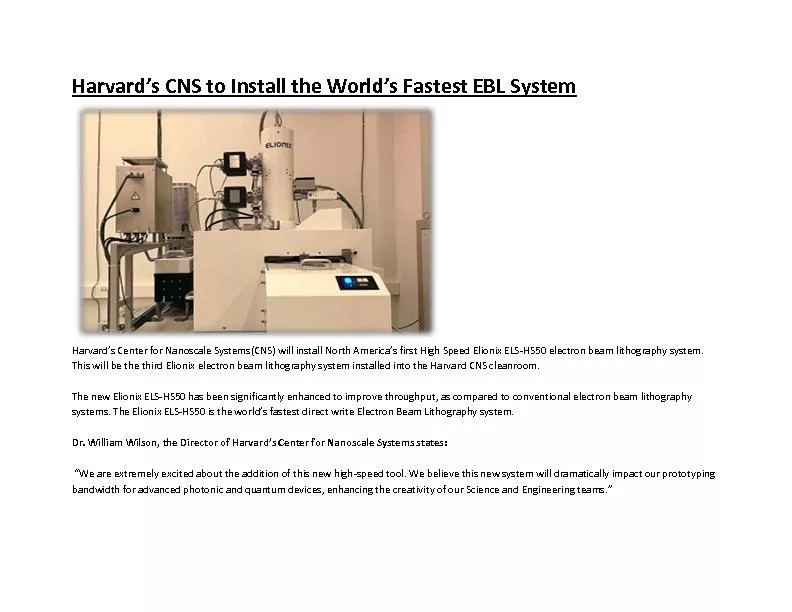
Harvard’s CNS to Install the World’s Fastest EBL System
by stselionix
Harvard’s Center for Nanoscale Systems(CNS) will...
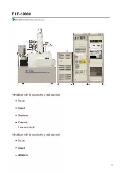
Electron Beam Lithography System - ELF 10000
by stselionix
Electron Beam Lithography System - ELF 10000
NE 353: Nano Probing and Lithography
by giovanna-bartolotta
Introduction.. Photon-based lithography: DUV (dee...
Ion Beam Lithography: Focused Ion Beam & Ion Projection Lithography
by conchita-marotz
Ziam Ghaznavi. CHE 384T Lithography. November 30....
Ion Beam Lithography: Focused Ion Beam & Ion Projection Lithography
by kittie-lecroy
Ziam Ghaznavi. CHE 384T Lithography. November 30....
Nanoscale Lithography, Techniques and Technology
by tawny-fly
EE 4611 . Dehua . liu. 4/8/2016. THE origin of Na...
Nanoscale Lithography, Techniques and Technology
by aaron
EE 4611 . Dehua . liu. 4/8/2016. THE origin of Na...
Lithography
by luanne-stotts
. kjetil. Lithography is the process of transfer...
Prof. Dr. Wisam J. Aziz
by LoveBug
Solid state physics. . Lecture (8). Nanolithograp...
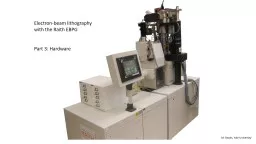
Electron-beam lithography
by tatiana-dople
with the . Raith. EBPG. Part 3: Hardware. M. Roo...
Electron-beam lithography
by briana-ranney
with the . Raith. EBPG. Part 3: Hardware. M. Roo...
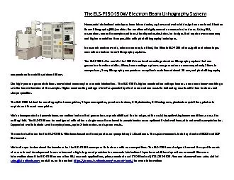
The ELS-F150 150kV Electron Beam Lithography System
by stselionix
Nanoscale fabrication techniques have taken device...
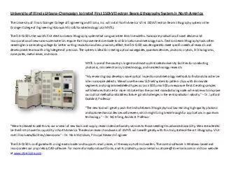
University of Illinois Urbana-Champaign to Install First 150kV Electron Beam Lithography System in North America
by stselionix
University of Illinois Urbana-Champaign to Install...
Nanoimprint lithography (NIL)
by myesha-ticknor
Overview.. Thermal NIL resists.. Residual layer a...
BY SURAJ MENON S7,EEE,61
by stefany-barnette
outline. Lithography. Introduction to EUVL. Basic...
UV-Curved
by alexa-scheidler
Nano. Imprint Lithography. Lithography. Imprint-...
M.C. Escher
by luanne-stotts
born: 1898 Leeuwarden, Holland. Background info. ...
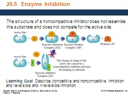
20.5 Enzyme Inhibition The structure of a noncompetitive inhibitor does not resemble the substrate
by BunnyBoo
.. Learning Goal . . Describe competitive and . n...
Substrate Preference and Mid-Mesozoic Brachiopod Decline
by pamella-moone
Marko Manojlovic . UC Santa Cruz. Brachiopods vs ...
Substrate permittivity
by debby-jeon
. measurement. . for. PCB. Printed. . Technol...
matched strain relaxed Lattice misfit Substrate Substrate Substrate Film Film Film fafasa sf Epitaxial Tilting of GaN Grown on Vicinal Surfaces of Sapphire Huang et
by alida-meadow
al brPage 8br bdf brPage 9br brPage 10br brPage 11...
The Effects of Substrate Composition on Intertidal Organism
by faustina-dinatale
Hala . Nader. , Alyson . Pickard, . Sam Shaw, &am...
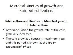
Microbial kinetics of growth and substrate utilization.
by sherrill-nordquist
Batch culture and Kinetics of Microbial growth in...
Electron-beam lithography
by sherrill-nordquist
Electron-beam lithography with the Raith EBPG P...
Electron-beam lithography
by mitsue-stanley
with the . Raith. EBPG. Part 1: Introduction. M....
Electron-beam lithography
by danika-pritchard
with the . Raith. EBPG. Part 1: Introduction. M....
ALLOSTERIC ENZYMES REGULATION
by franklin
By- . Shubhani. . singh. thakur. department of b...
Enzymes Learning Objectives:
by bodie278
1-. Describe . enzyme nomenclature. . 2-Explain t...
Higher Biology Unit 2 2.1 Metabolic Pathways & their Control
by drew
National . 5 Revision. Think!. In your jotter mak...
Factors Affecting Enzymatic Activity
by shepherd894
Enzyme Inhibition. Regulation of Enzyme Activity. ...
VBC-605 Unit II Enzyme kinetics
by briggs522
1. Enzyme concentration. 2. Temperature. 3. Hydrog...
Enzyme Inhibition By- Shubhani
by damon448
. singh. thakur. Department of biochemistry. Enzy...
ENZYMES Lecturer: 4
by theo509
Dr. . Shaimaa. . Munther. . ENZYMES : are effect...
Mechanism of enzyme action:
by hassan793
A. . Activation Energy:. 1.. . All the reactions ...
Veerashaiva College,
by isaiah
Ballari. . ( Affiliated to V.S.K....
Enzymes Enzymes are proteins
by judah
that . catalyze. (. i.e.. , . increase or decreas...
Load More...